
Multiple Switch Debouncer in VHDL
Project maintainers
Details
Created: Aug 9, 2011
Updated: May 22, 2017
SVN Updated: Sep 19, 2011
SVN: Browse
Latest version: download (might take a bit to start...)
Statistics: View
Bugs: 1 reported / 1 solved
Other project properties
Language:VHDL
Development status:Stable
Additional info:Design done, FPGA proven, Specification done
WishBone compliant: No
WishBone version: n/a
License: LGPL
Development Status
The core is tested and is being used in FPGA hardware in several projects.
Related Links
This core is being used in the SPI_MASTER_SLAVE verification test circuit: http://opencores.org/project,spi_master_slave
To get the latest version: http://opencores.org/download,debouncer_vhdl
If you have issues you like to be addressed, place a request in the bugtracker: http://opencores.org/project,debouncer_vhdl,bugtracker
If you find this core useful, please let me know: jdoin@opencores.org
If you find the LGPL license to be unfit for your purposes, please let me know and we can study changing the license to another open-source hardware license.
Description
This block is a general-purpose multiple input de-bouncing circuit.
It handles multiple inputs, like mechanical switch inputs, and outputs a de-bounced, stable registered version of the inputs.
A 'new_data' one-cycle strobe is also available, to sync downstream logic.
CONCEPTUAL CIRCUIT
The model has the generics N (input bus width) and CNT_VAL (clock counts for the de-bounce period).
                                        W
                       /----------------/----------------\
                       |                                 |
                       |                                 |
                       |        ______        ______     |         _____
                       |    W   |    |   W    |fdr |  W  |    W    |cmp \
                       \----/---| +1 |---/----|    |--/--+----/----|     \
                                |    |        |    |               |      \
                                ------        |    |               \       |
                                              |    |                |   =  |-----\
                                              |> R |               /       |     |
                                              ---+--               |      /      |
                                                 |       CNT_VAL---|     /       |
                                                 |                 |____/        |
                                                 |                               |
                                                 \------------\                  |
                                                              |                  |
                                   N    ____                  |                  |
                           /-------/---))   \      ____       |                  |
                           |           ))XOR |-----)   \      |                  |
                           |    /------))___/      )OR  |-----/                  |
                           |    |              /---)___/                         |
                           |    |              |                                 |
                           |    |              \----------\                      |
                           |    |        N                |                      |
                           |    \--------/-----------\    +----------------------+---------\
                           |                         |    |                                |
                           \---\                     |    |                                |
                  ______       |        ______       |    |   ______                       |
                  | fd |       |        | fd |       |    |   |fde |                       |
[data_i]----/-----|    |---/---+---/----|    |---/---+----)---|    |---/---+---/-----------)------------------------[data_o]
            N     |    |   N       N    |    |   N   |    |   |    |   N   |   N           |
                  |    |                |    |       |    \---|CE  |       |               |
                  |    |                |    |       |        |    |       |               |
[clk_i]---->      |>   |                |>   |       |        |>   |       |               |   ____       ______
                  ------                ------       |        ------       |   N    ____   \---|   \      | fd |
                                                     |                     \---/---))   \      |AND |-----|    |----[strb_o]
                                                     |                             ))XOR |-----|___/      |    |
                                                     \-------------------------/---))___/                 |    |
                                                                                N                         |    |
                                                                                                          |>   |
                                                                                                          ------
PIPELINE LOGIC
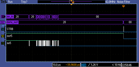
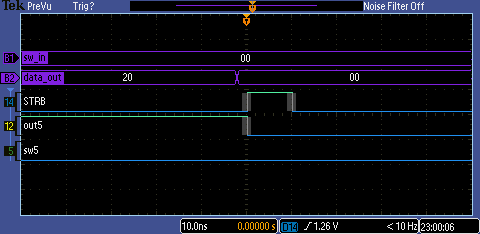
This de-bouncer circuit detects edges in an input signal, and waits the signal to stabilize for the designated time before transferring the stable signal to the registered output.A one-clock-cycle strobe is pulsed at the output to signalize a new data available.
The core clock should be the system high-speed clock, to optimize use of global clock resources, although a compromise may be met by using a lower frequency clock and a smaller counter for the de-bounce period. Care should be taken not to use a combinatorial clock, though, to avoid data setup time conflicts at the pipeline boundary.
GROUP DE-BOUNCING
A change in state in any bit in the input word causes reload of the delay counter, and the output word is updated only when all bits are stable for the specified period. Therefore, the grouping of signals and delay selection should match behavior of the selected signals.RESOURCES USED
Group de-bouncing saves area by having only one counter that is shared by all grouped signals.The number of registers inferred is: 3*N+(LOG(CNT_VAL)/LOG(2))+1 registers.
The number of LUTs inferred is roughly: ((4*N+2)/6)+3.
Slice distribution will vary, and depends on the control set restrictions and LUT-FF pairs resulting from map+p&r, but for groups of 8 signals the LUT-FF usage will be optimal.
This circuit is fully synthesizable and is written in technology-independent VHDL.
The design was originally targeted to a Spartan-6 platform, synthesized with XST and normal constraints, but contains no Xilinx-specific syntax or instantiated components.
Verification in silicon was done on a Digilent Atlys board with a Spartan-6 FPGA @100MHz clk_i.
The VHDL dialect used is VHDL'93, accepted largely by all synthesis tools.