Table of content
1. Introduction
The original MSP430 from TI provides a serial debug interface to allow
in-system software debugging. In that case, the communication
with the host computer is typically built on a JTAG or Spy-Bi-Wire
serial protocol. However, the global debug architecture from the MSP430
is unfortunately poorly documented on the web (and is also probably
tightly linked with the internal core micro-architecture).
A custom module has therefore been implemented for the
openMSP430. The communication with the host is done with a simple two-wire cable following either the UART or I
2C serial protocol (interface is selectable in the
Expert System Configuraiton section).
The debug unit provides all required features for Nexus Class 3 debugging (beside trace), namely:
Debug unit features
|
- CPU control (run, stop, step, reset).
- Software & hardware breakpoint.
- Hardware watchpoint.
- Memory read/write on-the-fly (no need to halt execution).
- CPU registers read/write on-the-fly (no need to halt execution).
|
Depending on the selected serial interface, the following features are available:
Debug interface features
|
UART
|
I2C
|
Strengths:
- No extra hardware required for most FPGA boards (almost all come with a UART interface, either RS232 or USB based).
- Possibility to use USB to serial TTL cables.
Weaknesses:
- Need to reset the debug interface after cable insertion.
- For ASICs, no possibility to change the MCLK frequency during a debug session.
|
Strengths:
- Very stable interface (synchronous protocol, no synchronization frame required).
- Multi-core chip support with a single I2C
interface (i.e. TWO pins)... in such a system, each openMSP430 instance has its own I2C device address.
- Possibility to combine the openMSP430 debug interface with
an already existing "functional" I2C interface... effectively creating
a ZERO
wire serial debug interface.
- Affordable USB-ISS adapter (~23€).
Weaknesses:
- Extra I2C adapter required (USB-ISS currently supported)
|
2. Debug Unit
2.1 Register Mapping
The following table summarize the complete debug register set accessible through the debug communication interface:
| Register Name |
Address |
Bit Field |
| 15 | 14 |
13 | 12 |
11 | 10 |
9 | 8 |
7 | 6 |
5 | 4 |
3 | 2 |
1 | 0 |
| CPU_ID_LO |
0x00 |
PER_SPACE |
USER_VERSION |
ASIC |
CPU_VERSION |
| CPU_ID_HI |
0x01 |
PMEM_SIZE |
DMEM_SIZE |
MPY |
| CPU_CTL |
0x02 |
Reserved |
CPU_RST |
RST_BRK_EN |
FRZ_BRK_EN |
SW_BRK_EN |
ISTEP |
RUN |
HALT |
| CPU_STAT |
0x03 |
Reserved |
HWBRK3_PND |
HWBRK2_PND |
HWBRK1_PND |
HWBRK0_PND |
SWBRK_PND |
PUC_PND |
Res. |
HALT_RUN |
| MEM_CTL |
0x04 |
Reserved |
B/W |
MEM/REG |
RD/WR |
START |
| MEM_ADDR |
0x05 |
MEM_ADDR[15:0] |
| MEM_DATA |
0x06 |
MEM_DATA[15:0] |
| MEM_CNT |
0x07 |
MEM_CNT[15:0] |
| BRK0_CTL |
0x08 |
Reserved |
RANGE_MODE |
INST_EN |
BREAK_EN |
ACCESS_MODE |
| BRK0_STAT |
0x09 |
Reserved |
RANGE_WR |
RANGE_RD |
ADDR1_WR |
ADDR1_RD |
ADDR0_WR |
ADDR0_RD |
| BRK0_ADDR0 |
0x0A |
BRK_ADDR0[15:0] |
| BRK0_ADDR1 |
0x0B |
BRK_ADDR1[15:0] |
| BRK1_CTL |
0x0C |
Reserved |
RANGE_MODE |
INST_EN |
BREAK_EN |
ACCESS_MODE |
| BRK1_STAT |
0x0D |
Reserved |
RANGE_WR |
RANGE_RD |
ADDR1_WR |
ADDR1_RD |
ADDR0_WR |
ADDR0_RD |
| BRK1_ADDR0 |
0x0E |
BRK_ADDR0[15:0] |
| BRK1_ADDR1 |
0x0F |
BRK_ADDR1[15:0] |
| BRK2_CTL |
0x10 |
Reserved |
RANGE_MODE |
INST_EN |
BREAK_EN |
ACCESS_MODE |
| BRK2_STAT |
0x11 |
Reserved |
RANGE_WR |
RANGE_RD |
ADDR1_WR |
ADDR1_RD |
ADDR0_WR |
ADDR0_RD |
| BRK2_ADDR0 |
0x12 |
BRK_ADDR0[15:0] |
| BRK2_ADDR1 |
0x13 |
BRK_ADDR1[15:0] |
| BRK3_CTL |
0x14 |
Reserved |
RANGE_MODE |
INST_EN |
BREAK_EN |
ACCESS_MODE |
| BRK3_STAT |
0x15 |
Reserved |
RANGE_WR |
RANGE_RD |
ADDR1_WR |
ADDR1_RD |
ADDR0_WR |
ADDR0_RD |
| BRK3_ADDR0 |
0x16 |
BRK_ADDR0[15:0] |
| BRK3_ADDR1 |
0x17 |
BRK_ADDR1[15:0] |
| CPU_NR |
0x18 |
CPU_TOTAL_NR |
CPU_INST_NR |
2.2 CPU Control/Status Registers
2.2.1 CPU_ID
This 32 bit read-only register holds the program and data memory size information of the implemented openMSP430.
| Register Name |
Address |
Bit Field |
| 15 | 14 |
13 | 12 |
11 | 10 |
9 | 8 |
7 | 6 |
5 | 4 |
3 | 2 |
1 | 0 |
| CPU_ID_LO |
0x00 |
PER_SPACE |
USER_VERSION |
ASIC |
CPU_VERSION |
| CPU_ID_HI |
0x01 |
PMEM_SIZE |
DMEM_SIZE |
MPY |
| | CPU_VERSION |
: Current CPU version
|
| | ASIC |
: Defines if the ASIC specific features are enabled in the current openMSP430 implementation. |
| | USER_VERSION |
: Reflects the value defined in the openMSP430_defines.v file. |
| | PER_SPACE |
: Peripheral address space for the current implementation (byte size = PER_SPACE*512) |
| | MPY |
: This bit is set if the hardware multiplier is included in the current implementation |
| | DMEM_SIZE |
: Data memory size for the current implementation (byte size = DMEM_SIZE*128) |
| | PMEM_SIZE |
: Progam memory size for the current implementation (byte size = PMEM_SIZE*1024) |
2.2.2 CPU_CTL
This 8 bit read-write register is used to
control the CPU and to configure some basic debug features. After a
POR, this register is set to 0x10 or 0x30 (depending on the
DBG_RST_BRK_EN configuration option).
| Register Name |
Address |
Bit Field |
| 7 | 6 |
5 | 4 |
3 | 2 |
1 | 0 |
| CPU_CTL |
0x02 |
Res. |
CPU_RST |
RST_BRK_EN |
FRZ_BRK_EN |
SW_BRK_EN |
ISTEP |
RUN |
HALT |
| | CPU_RST |
: Setting this bit to 1 will activate the PUC reset. Setting it back to 0 will release it. |
| | RST_BRK_EN |
: If set to 1, the CPU will automatically break after a PUC occurrence. |
| | FRZ_BRK_EN |
: If set to 1, the timers and watchdog are frozen when the CPU is halted. |
| | SW_BRK_EN |
: Enables the software breakpoint detection. |
| | ISTEP1 |
: Writing 1 to this bit will perform a single instruction step if the CPU is halted. |
| | RUN1 |
: Writing 1 to this bit will get the CPU out of halt state. |
| | HALT1 |
: Writing 1 to this bit will put the CPU in halt state. |
1:this field is write-only and always reads back 0.
2.2.3 CPU_STAT
This 8 bit read-write register gives the global status of the debug interface. After a POR, this register is set to 0x00.
| Register Name |
Address |
Bit Field |
| 7 | 6 |
5 | 4 |
3 | 2 |
1 | 0 |
| CPU_STAT |
0x03 |
HWBRK3_PND |
HWBRK2_PND |
HWBRK1_PND |
HWBRK0_PND |
SWBRK_PND |
PUC_PND |
Res. |
HALT_RUN |
| | HWBRK3_PND |
: This bit reflects if one of the Hardware Breakpoint Unit 3 status bit is set (i.e. BRK3_STAT≠0). |
| | HWBRK2_PND |
: This bit reflects if one of the Hardware Breakpoint Unit 2 status bit is set (i.e. BRK2_STAT≠0). |
| | HWBRK1_PND |
: This bit reflects if one of the Hardware Breakpoint Unit 1 status bit is set (i.e. BRK1_STAT≠0). |
| | HWBRK0_PND |
: This bit reflects if one of the Hardware Breakpoint Unit 0 status bit is set (i.e. BRK0_STAT≠0). |
| | SWBRK_PND |
: This bit is set to 1 when a software breakpoint occurred. It can be cleared by writing 1 to it. |
| | PUC_PND |
: This bit is set to 1 when a PUC reset occured. It can be cleared by writing 1 to it. |
| | HALT_RUN |
: This read-only bit gives the current status of the CPU:
|
| | |
0 - CPU is running.
1 - CPU is stopped.
|
2.2.4 CPU_NR
This 16 bit read only register gives useful information for multi-core systems.
| Register Name |
Address |
Bit Field |
| 15 | 14 |
13 | 12 |
11 | 10 |
9 | 8 |
7 | 6 |
5 | 4 |
3 | 2 |
1 | 0 |
| CPU_NR |
0x18 |
CPU_TOTAL_NR |
CPU_INST_NR |
| | CPU_TOTAL_NR |
: Total number of oMSP instances -1 (for multicore systems). |
| | CPU_INST_NR |
: Current oMSP instance number (for multicore systems). |
2.3 Memory Access Registers
The following four registers enable single and burst read/write access to both CPU-Registers and full memory address range.
In order to perform an access, the following sequences are typically done:
- single read access (MEM_CNT=0):
- set MEM_ADDR with the memory address (or register number) to be read
- set MEM_CTL (in particular RD/WR=0 and START=1)
- read MEM_DATA
- single write access (MEM_CNT=0):
- set MEM_ADDR with the memory address (or register number) to be written
- set MEM_DATA with the data to be written
- set MEM_CTL (in particular RD/WR=1 and START=1)
- burst read/write access (MEM_CNT≠0):
2.3.1 MEM_CTL
This 8 bit read-write register is used to control
the Memory and CPU-Register read/write access. After a POR, this
register is set to 0x00.
| Register Name |
Address |
Bit Field |
| 7 | 6 |
5 | 4 |
3 | 2 |
1 | 0 |
| MEM_CTL |
0x04 |
Reserved |
B/W |
MEM/REG |
RD/WR |
START |
| | B/W |
: 0 - 16 bit access. |
| | |
1 - 8 bit access (not valid for CPU-Registers). |
| | MEM/REG |
: 0 - Memory access. |
| | |
1 - CPU-Register access. |
| | RD/WR |
: 0 - Read access. |
| | |
1 - Write access. |
| | START |
: 0- Do nothing |
| | |
1 - Initiate memory transfer. |
2.3.2 MEM_ADDR
This 16 bit read-write register specifies the
Memory or CPU-Register address to be used for the next read/write
transfer. After a POR, this register is set to 0x0000.
Note: in case of burst (i.e. MEM_CNT≠0), this register
specifies the first address of the burst transfer and will be
incremented automatically as the burst goes (by 1 for 8-bit access and
by 2 for 16-bit access).
| Register Name |
Address |
Bit Field |
| 15 | 14 |
13 | 12 |
11 | 10 |
9 | 8 |
7 | 6 |
5 | 4 |
3 | 2 |
1 | 0 |
| MEM_ADDR |
0x05 |
MEM_ADDR[15:0] |
| | MEM_ADDR |
: Memory or CPU-Register address to be used for the next read/write transfer. |
2.3.3 MEM_DATA
This 16 bit read-write register gives (wr)
or receive (rd) the Memory or CPU-Register data for the next
transfer. After a POR, this register is set to 0x0000.
| Register Name |
Address |
Bit Field |
| 15 | 14 |
13 | 12 |
11 | 10 |
9 | 8 |
7 | 6 |
5 | 4 |
3 | 2 |
1 | 0 |
| MEM_DATA |
0x06 |
MEM_DATA[15:0] |
| | MEM_DATA |
: if MEM_CTL.WR - data to be written during the next write transfer. |
| | |
if MEM_CTL.RD - updated with the data from the read transfer |
2.3.4 MEM_CNT
This 16 bit read-write register controls the
burst access to the Memory or CPU-Registers. If set to 0, a single
access will occur, otherwise, a burst will be performed. The burst
being optimized for the communication interface, more details are given
there. After a POR, this register is set to 0x0000.
| Register Name |
Address |
Bit Field |
| 15 | 14 |
13 | 12 |
11 | 10 |
9 | 8 |
7 | 6 |
5 | 4 |
3 | 2 |
1 | 0 |
| MEM_CNT |
0x07 |
MEM_CNT[15:0] |
| | MEM_CNT |
: =0 - a single access will be performed with the next transfer. |
| | |
≠0 -
specifies the burst size for the next transfer (i.e number of data
access). This field will be automatically decremented as the burst goes. |
2.4 Hardware Breakpoint Unit Registers
Depending on the
defines
located in the "openmsp430_defines.v" file, up to four hardware
breakpoint units can be included in the design. These units can be
individually controlled with the following registers.
2.4.1 BRKx_CTL
This 8 bit read-write register controls the hardware breakpoint unit x. After a POR, this register is set to 0x00.
| Register Name |
Address |
Bit Field |
| 7 | 6 |
5 | 4 |
3 | 2 |
1 | 0 |
| BRKx_CTL |
0x08, 0x0C, 0x10, 0x14 |
Reserved |
RANGE_MODE |
INST_EN |
BREAK_EN |
ACCESS_MODE |
| | RANGE_MODE |
: 0 - Address match on BRK_ADDR0 or BRK_ADDR1 (normal mode) |
| | |
1 - Address match on BRK_ADDR0→BRK_ADDR1 range (range mode)
Note: range mode is not supported by the core unless the `DBG_HWBRK_RANGE define is set to 1'b1 in the openMSP430_define.v file. |
| | INST_EN |
: 0 - Checks are done on the execution unit (data flow). |
| | |
1 - Checks are done on the frontend (instruction flow). |
| | BREAK_EN |
: 0 - Watchpoint mode enable (don't stop on address match). |
| | |
1 - Breakpoint mode enable (stop on address match). |
| | ACCESS_MODE |
: 00 - Disabled |
| | |
01 - Detect read access.
10 - Detect write access.
11 - Detect read/write access
Note: '10' & '11' modes are not supported on the instruction flow |
2.4.2 BRKx_STAT
This 8 bit read-write register gives the status
of the hardware breakpoint unit x. Each status bit can be cleared by
writing 1 to it. After a POR, this register is set to 0x00.
| Register Name |
Address |
Bit Field |
| 7 | 6 |
5 | 4 |
3 | 2 |
1 | 0 |
| BRKx_STAT |
0x09, 0x0D, 0x11, 0x15 |
Reserved |
RANGE_WR |
RANGE_RD |
ADDR1_WR |
ADDR1_RD |
ADDR0_WR |
ADDR0_RD |
| | RANGE_WR |
:
This bit is set whenever the CPU performs a write access within the
BRKx_ADDR0→BRKx_ADDR1 range (valid if RANGE_MODE=1 and
ACCESS_MODE[1]=1). |
| | RANGE_RD |
:
This bit is set whenever the CPU performs a read access within the
BRKx_ADDR0→BRKx_ADDR1 range (valid if RANGE_MODE=1 and
ACCESS_MODE[0]=1).
Note: range mode is not supported by the core unless the `DBG_HWBRK_RANGE define is set to 1'b1 in the openMSP430_define.v file. |
| | ADDR1_WR |
:
This bit is set whenever the CPU performs a write access at the
BRKx_ADDR1 address (valid if RANGE_MODE=0 and ACCESS_MODE[1]=1). |
| | ADDR1_RD |
:
This bit is set whenever the CPU performs a read access at the
BRKx_ADDR1 address (valid if RANGE_MODE=0 and ACCESS_MODE[0]=1). |
| | ADDR0_WR |
:
This bit is set whenever the CPU performs a write access at the
BRKx_ADDR0 address (valid if RANGE_MODE=0 and ACCESS_MODE[1]=1). |
| | ADDR0_RD |
:
This bit is set whenever the CPU performs a read access at the
BRKx_ADDR0 address (valid if RANGE_MODE=0 and ACCESS_MODE[0]=1). |
2.4.3 BRKx_ADDR0
This 16 bit read-write register holds the value which is compared
against the address value currently present on the program or data
address bus. After a POR, this register is set to 0x0000.
| Register Name |
Address |
Bit Field |
| 15 | 14 |
13 | 12 |
11 | 10 |
9 | 8 |
7 | 6 |
5 | 4 |
3 | 2 |
1 | 0 |
| BRKx_ADDR0 |
0x0A, 0x0E, 0x12, 0x16 |
BRK_ADDR0[15:0] |
| | BRK_ADDR0 |
: Value compared against the address value currently present on the program or data address bus. |
2.4.4 BRKx_ADDR1
This 16 bit read-write register holds the
value which is compared against the address value currently present on
the program or data address bus. After a POR, this register is set to
0x0000.
| Register Name |
Addresses |
Bit Field |
| 15 | 14 |
13 | 12 |
11 | 10 |
9 | 8 |
7 | 6 |
5 | 4 |
3 | 2 |
1 | 0 |
| BRKx_ADDR1 |
0x0B, 0x0F, 0x13, 0x17 |
BRK_ADDR1[15:0] |
| | BRK_ADDR1 |
: Value compared against the address value currently present on the program or data address bus. |
3. Debug Communication Interface: UART
With its UART interface,
the openMSP430 debug unit can communicate with the host computer using
a simple RS232 cable (connected to the
dbg_uart_txd and
dbg_uart_rxd ports of the IP).
Typically, a
USB to RS232 or
USB to serial TTL
cable will provides a reliable communication link between your host PC
and the openMSP430 (speed being typically limited by the cable length).
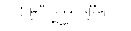
3.1 Serial communication protocol: 8N1
There are plenty tutorials on Internet regarding RS232 based protocols.
However, here is quick recap about 8N1 (1 Start bit, 8 Data bits, No
Parity, 1 Stop bit):

As you can see in the above diagram, data transmission starts with a
Start bit, followed by the data bits (LSB sent first and MSB sent
last), and ends with a "Stop" bit.
3.2 Synchronization frame
After a POR, the Serial Debug
Interface expects a synchronization frame from the host computer in
order to determine the communication speed (i.e. the baud rate).
The synchronization frame looks as following:
As you can see, the host simply sends the 0x80 value. The openMSP430
will then measure the time between the falling and rising edge, divide
it by 8 and automatically deduce the baud rate it should use to
properly communicate with the host.
Important note: if you want to change the communication speed
between two debugging sessions, the Serial Debug Interface needs to go through a reset cycle (i.e. through the
reset_n or
dbg_en pins) and a new synchronization frame needs to be send.
3.3 Read/Write access to the debug registers
In order to perform a read / write access to a debug register, the host needs to send a command frame to the openMSP430.
In
case of write access, this command frame will be followed by 1 or 2
data frames and in case of read access, the openMSP430 will send 1 or 2
data frames after receiving the command.
3.3.1 Command Frame
The command frame looks as following:

| | WR |
: Perform a Write access when set. Read otherwise. |
| | B/W |
: Perform a 8-bit data access when set (one data frame). 16-bit otherwise (two data frame). |
| | Address |
: Debug register address. |
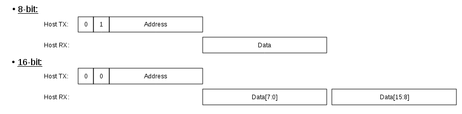
3.3.2 Write access
A write access transaction looks like this:
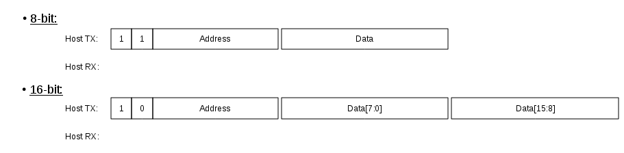
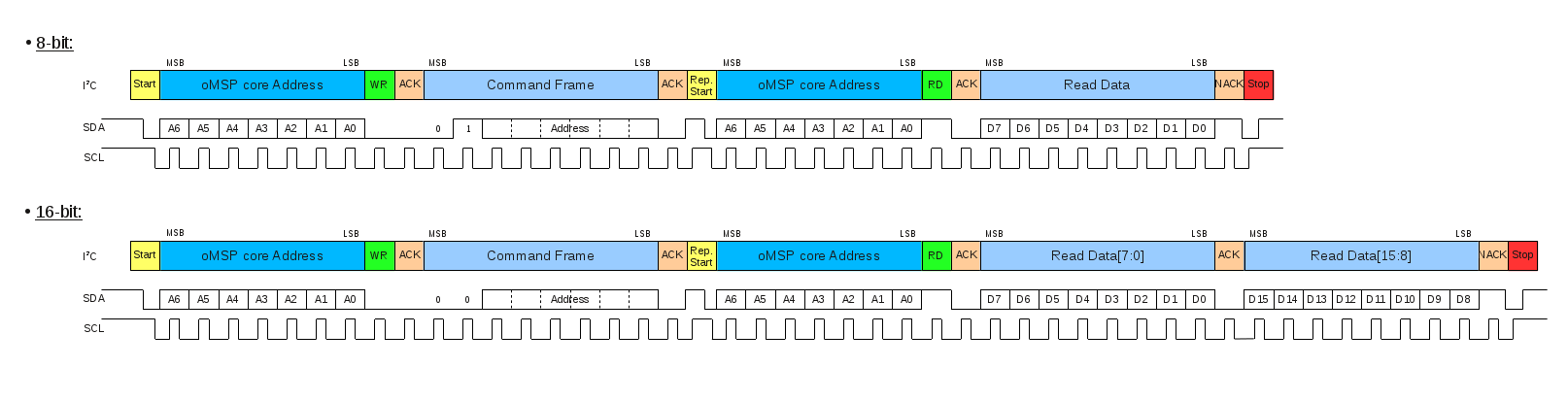
3.3.3 Read access
A read access transaction looks like this:
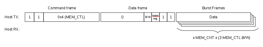
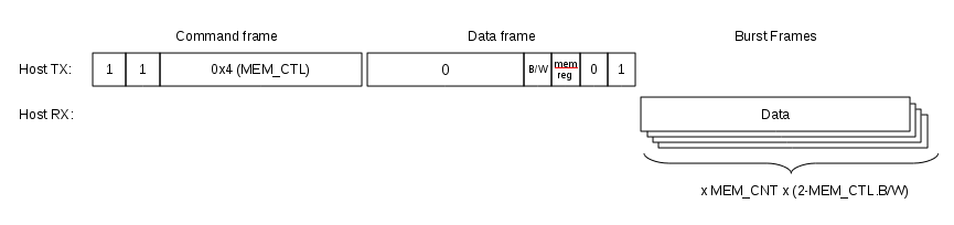
3.4 Read/Write burst implementation for the CPU Memory access
In
order to optimize the data burst transactions for the UART, read/write
access are not done by reading or writing the MEM_DATA register.
Instead, the data transfer starts immediately after the MEM_CTL.START bit has been set.
3.4.1 Write Burst access
A write burst transaction looks like this:
3.4.2 Read Burst access
A read burst transaction looks like this:
4. Debug Communication Interface: I2C
With its I2C interface, the openMSP430 debug unit can communicate with the host computer using
an I2C adapter (connected to the
dbg_i2c_scl and
dbg_i2c_sda_in / dbg_i2c_sda_out ports of the IP).
Currently, the
USB-ISS
adapter from Devantech (Robot Electronics) is supported by the software
development tools and provides a reliable communication link between
your host PC
and the openMSP430.
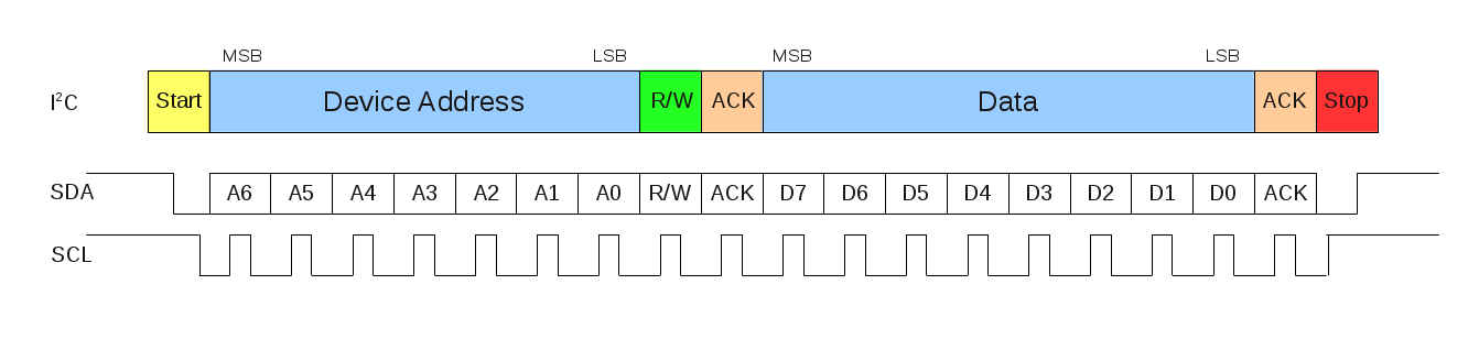
4.1 I2C communication protocol
There are plenty tutorials on Internet regarding the I2C protocol (see the official
I2C specification for more info).
A simple byte read or write frame looks as following:
4.2 Synchronization frame
Unlike the UART interface, the I2C is a synchronous communication protocol.
A synchronization frame is therefore not required.
4.3 Read/Write access to the debug registers
In order to perform a read / write access to a debug register, the host needs to send a command frame to the openMSP430.
In
case of write access, this command frame will be followed by 1 or 2
data frames and in case of read access, the openMSP430 will send 1 or 2
data frames after receiving the command.
4.3.1 Command Frame
The command frame looks as following:
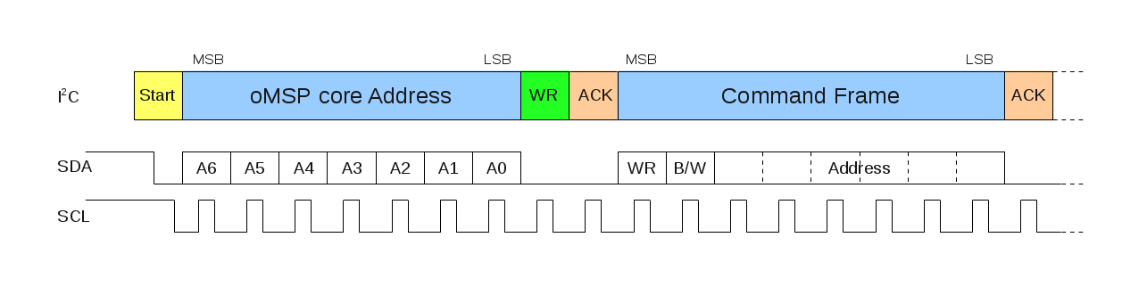
| | WR |
: Perform a Write access when set. Read otherwise. |
| | B/W |
: Perform a 8-bit data access when set (one data frame). 16-bit otherwise (two data frame). |
| | Address |
: Debug register address. |
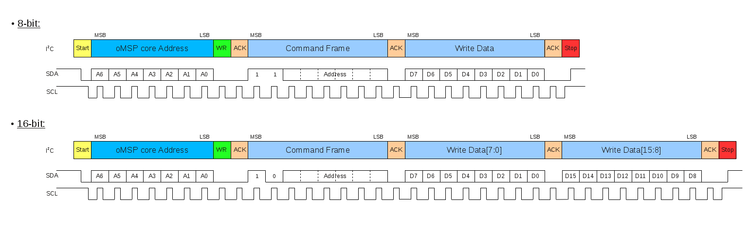
4.3.2 Write access
A write access transaction looks like this:
4.3.3 Read access
A read access transaction looks like this:
4.4 Read/Write burst implementation for the CPU Memory access
In
order to optimize the data burst transactions for the I2C, read/write
access are not done by reading or writing the MEM_DATA register.
Instead, the data transfer starts immediately after the MEM_CTL.START bit has been set.
4.4.1 Write Burst access
A write burst transaction looks like this:
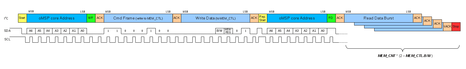
4.4.2 Read Burst access
A read burst transaction looks like this:

 openMSP430