
SHA256 HASH CORE
Project maintainers
Details
Created: Jul 14, 2016
Updated: Mar 7, 2019
SVN Updated: Oct 15, 2016
SVN: Browse
Latest version: download (might take a bit to start...)
Statistics: View
Bugs: 0 reported / 0 solved
Other project properties
Language:VHDL
Development status:Stable
Additional info:
WishBone compliant: No
WishBone version: n/a
License: LGPL
PROJECT UPDATES
The OpenCores SVN is back online. The project is up-to-date.
If you have any problem donwloading, please email me at jdoin@opencores.org
Development Status
The VHDL code is functional, tested and verified at the RTL synthesis level.
Hardware verification and performance characterization will follow.
FPGA performance tests show synthesis at 80MHz top clock speed. At 74MHz, the engine runs 580Mbps.
The project will include source code for an ARM LPC1768 mbed board testing a Spartan-6 Atlys board with the GV_SHA256 core under test, using parallel ports to test the SHA256 engine performance.
The hardware verification project will also encapsulate the GV_SHA256 in a fast SPI wrapper for functional testing, as an external SHA256 engine interfaced by a fast SPI bus.
SHA256 algortihm
The SHA256 hash is a block transformation algorithm based on LFSR message expansion.
The algorithm has 2 parts: the Message Schedule and the Hash Core.
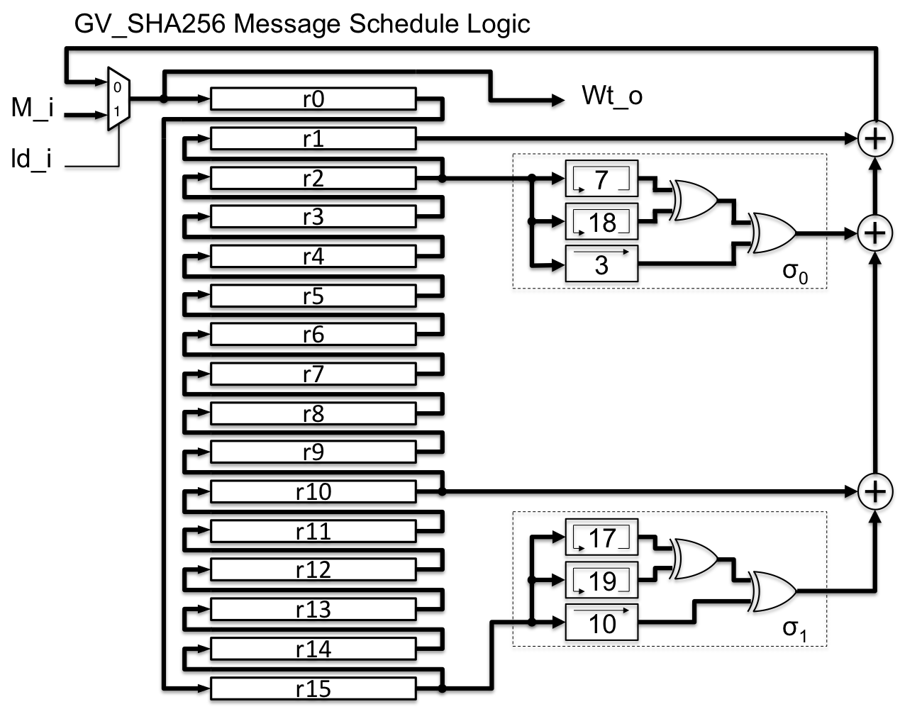
The message schedule can be implemented as a compact 16-word circular buffer, that is cycled for the 64 clock cycles.
Here is a simplified diagram of our implementation of the message schedule datapath, with the circular buffer (r0 .. r15) and the combinational functions (σ0, σ1).
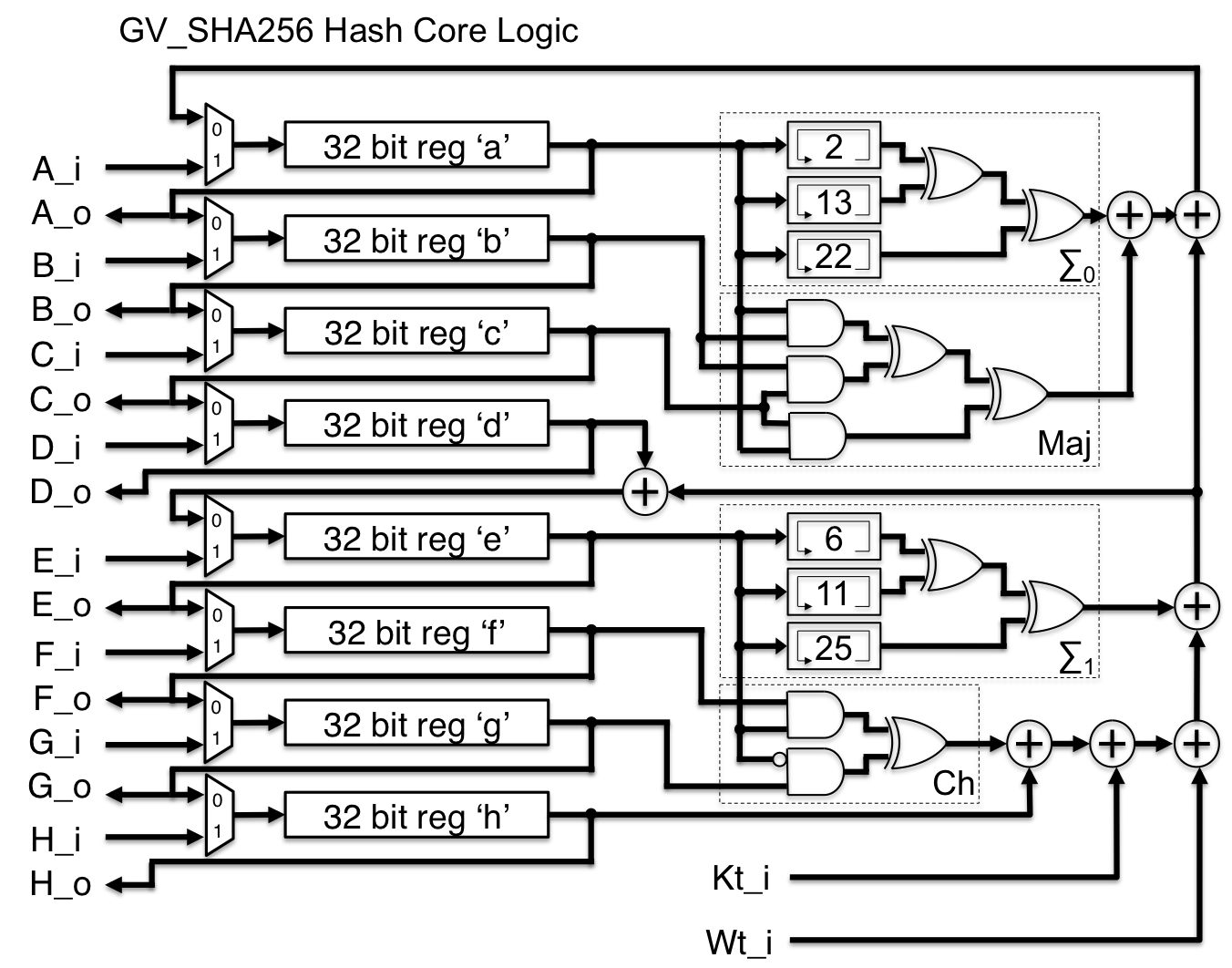
We implement the core logic as a word-shift register with combinational logic that computes the next state for the word shifter registers.
Here is a simplified depiction of the hash core logic datapath, with the core registers (a .. h) and the combinational functions (Maj, Ch, ∑0, ∑1).
The whole block is processed in a single clock cycle for each of the 64 cycles of the algorithm.
Note on the combinational functions (Maj, Ch, ∑0, ∑1, σ0, σ1): The sigma functions shifters are implemented as fixed bit remap (zero-logic), and the Maj and Ch are canonical implemetations of the FIPS-180-4 description. These boolean functions can be rearranged to match the target gates library. For LUT-based FPGA targets, the boolean remap saves no area, but for ASIC targets and more limited FPGA sea of gates, the remap can save combinational depth.
Note on the wide port adders: The hash algorithm is heavily dependent on adder architecture. When implemented with 2-port 32+32 bit adders, a cascade of adders can be used for the adder chain, reducing interconnect complexity. However, aggressive implementation with wide port parallel adders can reduce combinational path length and increase top clock rates, at the expense of interconnect and area constraints.
Description
This is the GV_SHA256, a fast SHA-256 engine (580Mbps @ 74MHz), fully compliant to the NIST FIPS-180-4 SHA-256 approved algorithm.
It is implemented as a single-cycle combinational logic for one iteration of the hash core, with a total of 65 clocks for the full 512-bit block hash operation.
The design is fully static, with a clean data path / control path approach.
The core has minimal registers, and is a parallel 256-bit processor, that receives a stream of 32-bit words, and delivers a 256-bit parallel hash output.
Interfacing with the engine is easy, with flow control signals that facilitate bus interfacing.
The testbench includes NIST vectors to verify against all corner cases for the SHA256 algorithm and block padding.
This logic synthesizes to system clocks of 72MHz, with ~10 layers of longest combinational logic path, without pipelining, in Spartan-6 (speed grade 2) technology.
The main objective is to share the design in order to benefit from the process Verification in several technologies, and maybe get feedback on design glitches for the algorithm optimizations. The implementation is straightforward, with aspect naming after the NIST-180-4 source description, and is optimized for minimum registers, instead of for minimum combinational length. That is a good fit for IoT applications, where silicon area may be more important than maximum clock speed.
I have more aggressively optimized versions of the SHA256 family (HMAC_SHA256, HKDF, DRBG), used on our closed-source cyber security ASICs.
Algorithm optimizations and parallel adder optimizations reduce the cycles per function and increase the top clock speeds of these crypto functions.
This core is the base of the GridVortex Crypto Library, for HMAC-SHA256, HMAC-SHA256-DRBG, HKDF and HMAC-DRBG-KDF cryptographic constructions.
The VHDL is written as hand-optimized RTL targeted for ASIC processes, especially IoT ASICs at 130nm/90nm.
However, it is easily integrated on FPGA targets. No FPGA hard logic are used in the description.
All feedback are highly appreciated.