Next 80186 processor
Project maintainers
Details
Created: Mar 12, 2012
Updated: May 31, 2013
SVN Updated: May 13, 2014
SVN: Browse
Latest version: download (might take a bit to start...)
Statistics: View
Bugs: 0 reported / 0 solved
Other project properties
Language:Verilog
Development status:Stable
Additional info:FPGA proven, Specification done
WishBone compliant: No
WishBone version: n/a
License: LGPL
Description
80186 instruction compatible, high performance processor, able to execute up to 40MIPS on a Spartan3AN FPGA. It requires ~1500 slices (25%) on a Spartan3AN. The speed performance is comparable with a 486 in 16bit real mode.
Features
Next186 CPU features:
- All 80186 intstructions are implemented according with the 80186 specifications (excepting ENTER instruction, which uses always 0 as the second parameter - level).
- all 80186 exceptions implemented (divide error - INT0, Trace - INT1, Overflow - INT4, Bounds - INT5, Invalid opcode - INT6, Coprocesor exception - INT7)
- Mascable and non mascable interrupts implemented. If a repeat block instruction is interrupted, the return address is the repeated instruction including all prefixes. This allows fully resume of repeated instruction after interrupt, with no other precautions.
- Designed with 2 buses: 16bit data / 20bit data_address and 48bit instruction / 20bit instruction_address. This allows most instructions to be executed in one clock cycle.
- In order to link the CPU unit on a single memory bus, these sepparate data/instruction buses must be multiplexed by a dedicated bus interface unit (BIU).
- It is able to execute up to 40 MIPS on Spartan XC3S700AN speed grade -4, performances comparable with a 486 CPU (real mode, 16bit only).
- Small size, the CPU + BIU requires ~25% or 1500 slices - on Spartan XC3S700AN
Next186 BIU (Bus Interface Unit) features:
- Links the CPU with a 32bit static synchronous RAM (or cache)
- Able to address up to 1MB
- 16byte instruction prefetch queue
- Works at 2 X CPU frequency (80Mhz on Spartan3AN), requiring minimum 2T for an instruction.
- The 32bit data bus and the double CPU clock allows the instruction queue to be almost always full, avoiding the CPU starving. The data un-alignement penalties are required only when data words crosses the 4byte boundaries.
Instruction timing
How to compute each instruction duration, in BIU clock cycles:
1 - From the Next186_features.doc see for each instruction how many CPU T states are required (you will notice they are always
less or equal than 486 and much less than the original 80186)
2 - Multiply this number by 2 - the BIU works at double CPU frequency because it needs to multiplex the data and instructions,
in order to keep the CPU permanently fed with instructions.
3 - Add penalties, as follows:
+1T for each memory read - because of the synchronous SRAM which need this extra cycle to deliver the data
+2T for each jump - required to flush and re-fill the instruction queue
+1T for each 16bit(word) read/write which overlaps the 4byte boundary - specific to 32bit bus width
+1T if the jump is made at an address with the latest 2bits 11 - specific to 32bit bus width
+1T when the instruction queue empties - this case appears very rare, when a lot of 5-6 bytes memory write instructions are executed in direct sequence
Some examples:
- "lea ax,[bx+si+1234]" requires 2T
- "mov word ptr [bx+si+1234],5678" requires 2T
- "add ax, 2345" requires 2T
- "xchg al, [bx]" requires 4T
- "inc word ptr [1]" requires 5T (2x2T inc M + 1T read)
- "inc word ptr [3]" requires 7T (2x2T inc M + 1T read + 1T unaligned read + 1T unaligned write)
- "imul ax,bx,234" requires 4T (2x2T imul)
- "loop address != 3(mod 4)" requires 4T/2T (2x1T loop + 2T flush if jump)
- "loop address == 3(mod 4)" requires 5T/2T (2x1T loop + 2T flush if jump + 1T unaligned jump)
- "call address 0" requires 4T (2x1T call near + 2T flush
- "ret address 0" requires 7T (2x2T ret + 1T read penalty + 2T flush)
Testbench
The package contains a minimal demonstration system containing:
- Next80186 CPU
- Next80186 BIU - 32bit bus, 80Mhz (the clock can be easily modified by tuning the DCM - but you also need to adjust the bootstrap RS232 receiver code which uses delays made with loop).
- 4KB SRAM (2KB at address 00000h - interrupt vector zone, 2KB at address FF800h - ROM zone)
- 1DCM with 50Mhz input and 80Mhz output
The system is connected to RS232, to 9 LEDs on board and to a RESET button.
The SRAM is preloaded with a RS232 (115200bps) bootstrap able to load and run an executable at address FF80:0100.
A sample .ASM application is provided (a simple RS232 feedback loop, with a mini memory dump feature).
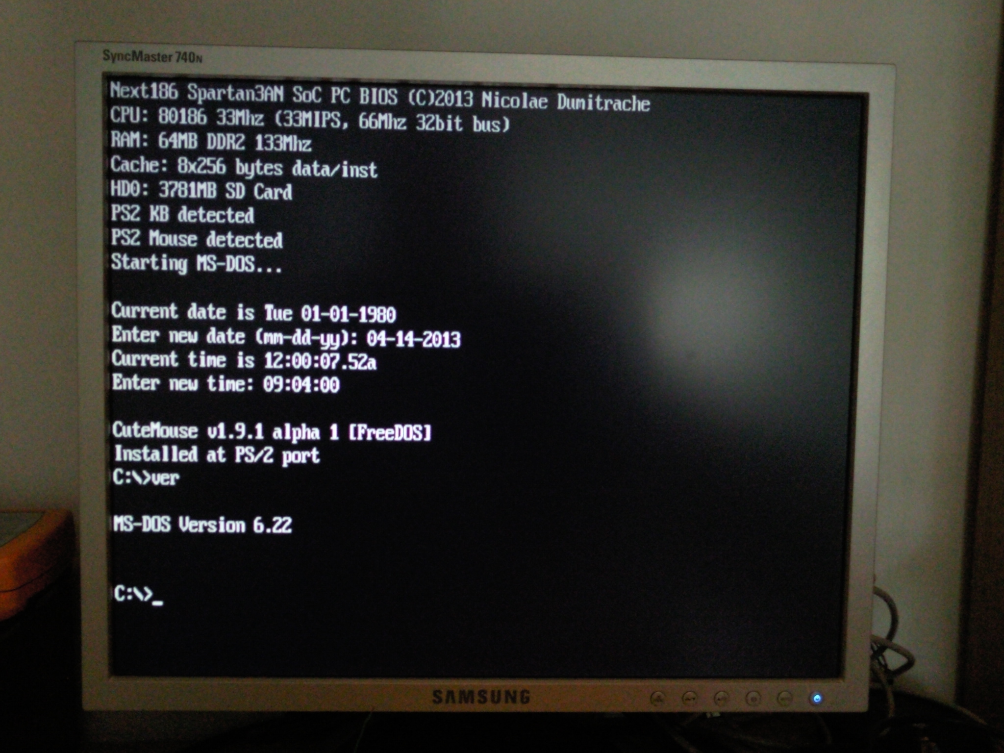
PC AT SoC - Running MS DOS 6.22
Booting DOS 6.22 on a Next186 PC AT SoC Xilinx Spartan 3AN used at ~50%
(64MB DDR2, simplified VGA, PS2 KB and mouse, SDCard 4GB, 33MIPS, speaker sound)
NC V5.0

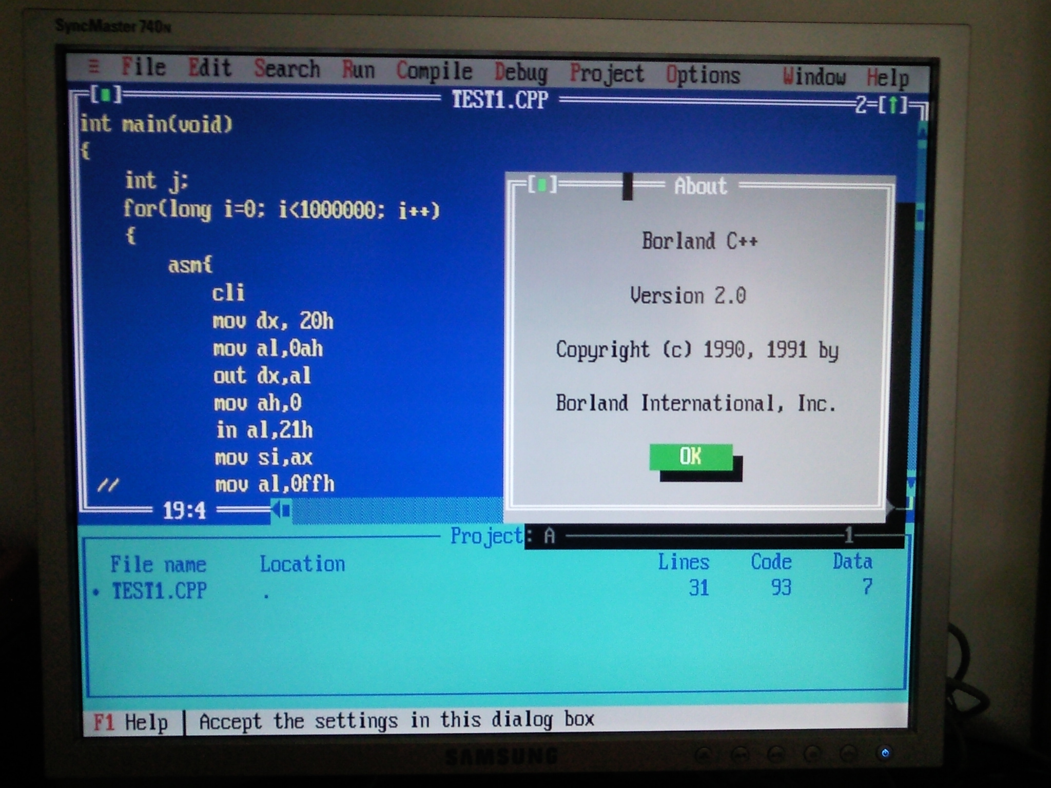
Running BC++ v2.0
Running Turbo Pascal 7

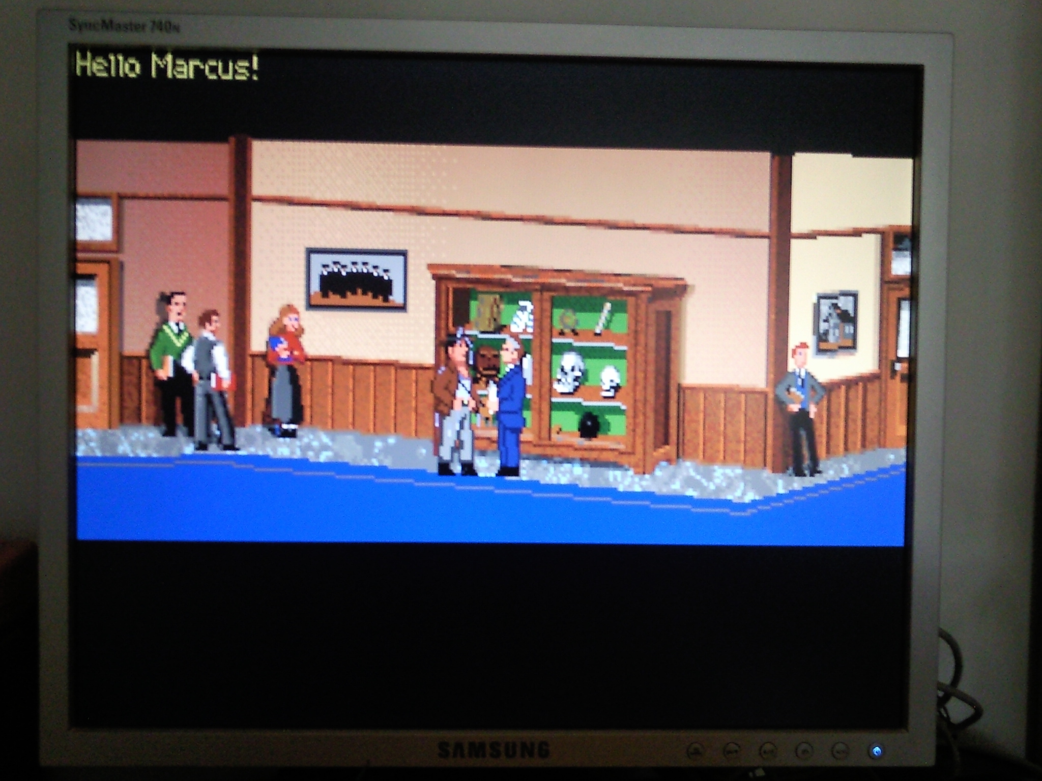
Indy MCGA
Prince of Persia 2 MCGA

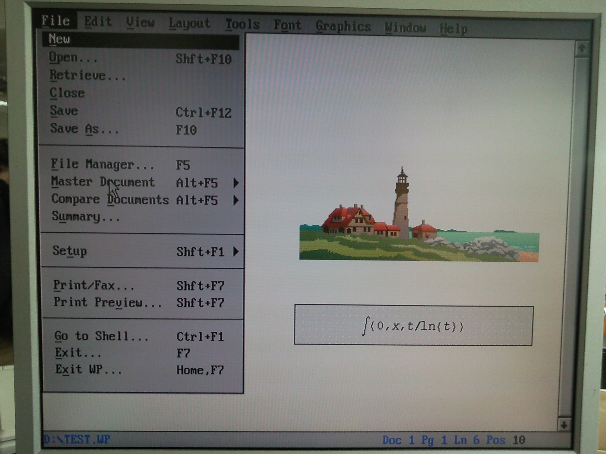
WordPerfect 6.0 in 640x480x256
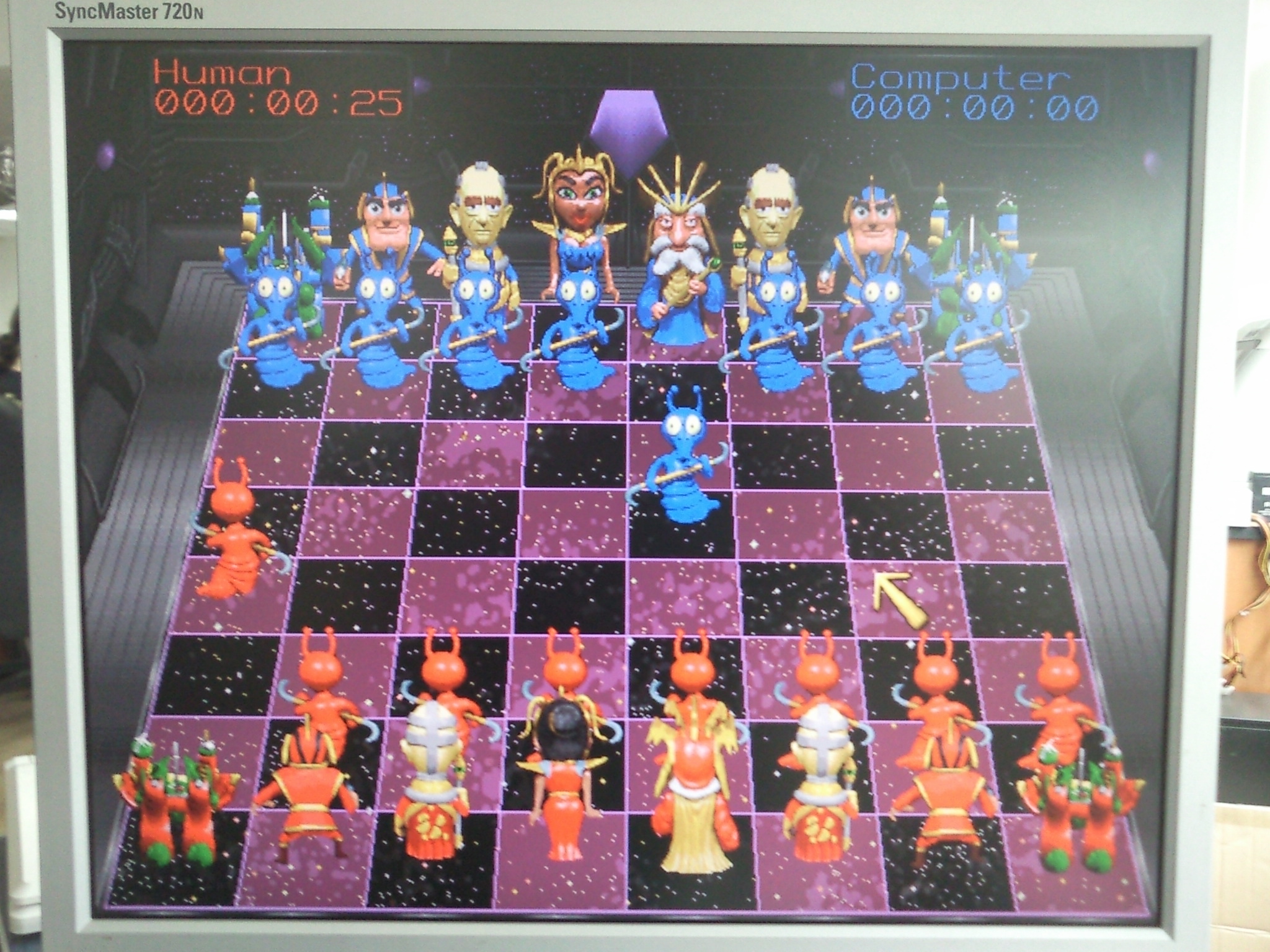
BattleChess4000 in 640x480x256, using EMM

