
Wishbone DDR3 SDRAM Controller
Project maintainers
Details
Created: Jul 27, 2016
Updated: Sep 17, 2016
SVN Updated: Aug 23, 2019
SVN: Browse
Latest version: download (might take a bit to start...)
Statistics: View
Bugs: 0 reported / 0 solved
Other project properties
Language:Verilog
Development status:Planning
Additional info:Specification done
WishBone compliant: Yes
WishBone version: n/a
License: GPL
Description
The purpose of this core is to provide a GPL wishbone core capable of commanding a DDR3 memory, such as the one used on Digilent's Arty board, at full speed. A particular design goal is that consecutive reads or writes should take only one additional clock cycle per read or write. My eventual goal is to build this so that it will support my OpenArty project.
Since the DDR3 memory specification is dated August, 2009, memory chips have been built to this specification. However, since the DDR3 SDRAM's are rather complex, and there is a lot of work required to manage them, controllers for DDR3 SDRAM's are primarily in the realm of proprietary.
Currently, as of this posting (20160728), there are no DDR3 SDRAM controllers on OpenCores. Sure, there's a project named DDR3 SDRAM controller, yet it has no data files present with it. This leaves an FPGA engineer with the choice of building a controller for a very complex interface from scratch, or using a proprietary core from Xilinx's Memory Interface Generator (MIG--assuming Xilinx is being used), for which there is no insight into how it works, and then retooling their bus from wishbone to AXI.
This core is designed to meet that need: it is both open (GPL), as well as wishbone compliant. Further, this core offers 32--bit granularity to an interface that would otherwise offer only 128-bit granularity. This core also offers complete pipelined performance. Because of the pipeline performance, this core is appropriate for filling cache lines. Because the core also offers non-pipelined performance, it is also appropriate for random access from a CPU-whether by a write-through cache or a CPU working without a cache.
Current Status
As anyone who has worked with DDR3 memory controllers will know, this is a difficult and complex project. There are lots of parts and pieces to it. Currently, a large portion (not all) of the Verilog code has been built, together with what should be a very thorough Verilator test bench. The Verilator code successfully brings the memory out of a reset condition, and starts its first write command. The next step will be completing this write command, and finishing the read logic.
Watch this space, if you are interested.
20160730 Update:
They say success is measured by the number of failures/redesigns along the way. If this is the case, I'm still a couple of failures away from success. I rebuilt the entire refresh logic today. It's by no means optimal, but should be reliable. (It lasts through one round in the simulator--it's within a clock or two of getting the second refresh right.) I'm also going to need to rebuild/redesign the command logic into a proper pipeline with stalls along the way in order to meet my goals. This is just life and where I'm at.The good news is that reset works, as do single 32-bit value writes (in the included Verilator simulation ...)
The other good news is that I should be able to calculate timing. So, if you wish to write N adjacent values in a pipelined fashion, the amount of time it will take will be between 55+5N (ns) and 95+5N (ns), depending upon whether or not the corresponding bank is open at the write or wrong value.
20160801 Update:
The controller now passes all of my simulation tests. It builds within Vivado as a part of the OpenArty project. Further testing, though, is sadly going to be limited to singular writes and minor pipeline reads until my OpenArty design has a CPU sufficient enough to prove that it works.20160802 Update:
So today was cleanup day. I dug into the spec to learn about all those things I didn't understand before. As a result, the ODT signal is (now) properly implemented, as is the write-to-precharge and write-to-read delays. There's a read-to-write delay that's not enforced, but I don't think the WB bus would let that happen. I also discovered I was using the wrong clock when building within Vivado, and moving from a 160MHz clock to a 200MHz clock exposed some timing problems. These have all been fixed.I also learned more about Xilinx's ODDR and IDDR primitives, and so I fixed some bugs there.
This leaves me with two problems: 1) Fixing the timing issue broke the simulation, and 2) while testing at 160MHz without the timing fix, the answers and results from the memory were all over the map. I may be able to read and write 1/16 times, and I can't explain why that one time works.
Tomorrow, I shall try to see if I can't user an iserdese2 as a logic analyzer to see what's really going on---once I get the simulation logic fixed (again).
20160803 Update:
Well, I didn't go for the ISERDESE2 (yet). I went back over the DDR3 spec, reread things, noticed things I had missed, and then started implementing more criteria into the simulator that the code was supposed to pass. When it didn't pass, I redesigned how activates and precharges are handled, and worked at it again. The good news is that it works in the simulation again. The good news is also that it looks more reasonable on the hardware than it did before (I had the PLL turned off before, oops). The bad news is that, on the hardware, there's still a decay problem: values set to 1's decay to 0's over time. So, there must still be something wrong in the refresh logic.20160805 Update:
Looks like I made some massive miscalculations in timing. The DDR1600 memory that I'm trying to command will accept commands at an 800MHz rate, not the 200MHz rate that I had thought. Further, since I don't think I can get my logic up to that speed, and yet since I still want to support the memory at full speed, that means I need to rethink my approach. In particular, I think I'm going to need to do a lot more in parallel. My goal remains to be able to run the memory at it's full speed, it's just ... that speed has now changed due to my misunderstanding of it. Full speed is 128-bits per 5ns (200MHz) clock, not 32-bits per 5ns clock. Since I like running my bus width at 32-bits, I'm still going to want to be able to run this at 32-bits per clock, but I'll also want to run it at 128 bits per clock as well.At any rate, I'm scratching my head on the drawing board right now. Since the commands must be issued in parallel, it makes sense to reserve timeslots for each command: The first could be reserved for Write, then Read, then Activate (open), then Precharge. This would allow precharge to be followed by an activate 11 clocks later, followed by a read, followed by a full vector-width read, as in:
| Clk | TS1 | TS2 | TS3 | TS4 | Internal | Bus |
|---|---|---|---|---|---|---|
| 1 | NOOP | NOOP | NOOP | NOOP | Idle | Active |
| 2 | NOOP | NOOP | NOOP | NOOP | Registered | (Idle, or stalled if active) |
| 3 | NOOP | NOOP | NOOP | Pre-Charge | Stalled | |
| 4 | (2) | (3) | (4) | (5) | Stalled | |
| 5 | (6) | (7) | (8) | (9) | Stalled | |
| 6 | (10) | (11) | Activate | (2) | Stalled | |
| 7 | (3) | (4) | (5) | (6) | Stalled | |
| 8 | (7) | (8) | (9) | (10) | Stalled | Potential next bus command |
| 9 | (11) | READ | (2) | (3) | Next Cmd | (Idle) |
| 10 | (4) | (5/nxt read?) | (6) | (7) | ||
| 11 | (8) | (9) | (10) | (11) | ||
| 12 | 128-bit Data Transfer | |||||
| 13 | (Determined by next command, otherwise idle) | ACK, and data returned | ||||
This is my plan going forward, but it may mean that I have to scrap a lot of what I've done.
20160816 Update:
I'm starting over. The WBDDR3 module needs to be totally rewritten, although it looks like I can salvage the reset and refresh logic from the previous version. I might even manage to salvage the simulation, and just call it 4 times per Verilator clock evaluation. After that, most everything is going to need to be rewritten.I've spent my time going back over the specification and marking it up. As I last mentioned, I'll need to run this with a 1.25ns clock. That means that we can transfer 128 bits per clock on the data lines. It also means that, if this core is to run with a 5ns clock, that the core will issue four commands to the memory at any given 5ns clock. Some pictures might help explain that. First is a picture showing what a read will look like:
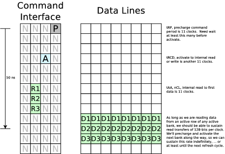
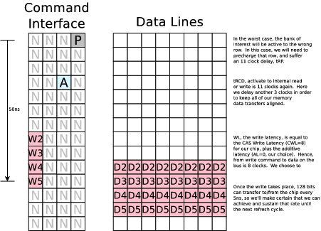
Here's another diagram showing what a write will look like. Notice the two sets of columns. The first is the command column, consisting of four 1.25ns commands per 5ns clock. A "P" is a pre-charge command, an "A" is an activate command, a "N" is a NOOP, a "Wx" is a write command, and a "Rx" is a read command, and so forth. Later, we'll use "R" to refer to a refresh command.
Our last image shows a refresh cycle:
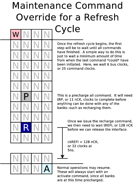
I'm developing other, similar, images to understand how the timing will play out from one command to the next, but those aren't nearly as pretty to show at this time.
20160818 Update:
As if this project wasn't difficult enough on its own, I seem to be making it more difficult. In particular, the Arty platform has a DDR3-1333 (9-9-9) memory, not the DDR3-1600 (11-11-11) memory that I was designing a solution for. This offers some particular problems. First, I have arbitrarily chosen an FPGA clock rate of 200MHz. This was originally chosen to support the DDR1600, because I (erroneously) thought that a DDR1600 memory would transfer 32-bits per clock if my clock was 200MHz. (This is my goal, 32-bits per clock at 200 MHz.) Still, if I'm using a 200MHz FPGA clock, I can't expand by 4 parallel commands as I could with the DDR1600. (First two commands are column specific, last two row specific--logic gets simplified--only this doesn't work ... Grr.) So, what choice do I have? I can run the memory with a 600MHz clock. That would mean I'd have to do the logic for three commands in parallel, and I would read 96 of 128 bits per clock. The problem is, it would be difficult to schedule the instructions when the data doesn't regularly start at the top of the clock. Alternatively, I could run the memory with a 400MHz command clock, run the whole interface at 2x parallel, and get 64 bits of data transferred per clock. This latter approach is going to be my approach going forward.Hence a read is going to look like (now)
20160819 Update:
Remember when I said that the controller passed all simulation tests I could give it? Well, we've gotten back to that point--the simulation and core have both been updated to match the specification, as best I understand it (now). So I just posted new and updated code to the repository. It works in simulation (again), although the calling convention has changed somewhat. The core can now handle, barring refresh cycles, 64-bit reads or writes in a pipelined fashion on every cycle. This is overkill for my needs (32-bit read/writes on every cycle), but there are others who will want this extra capability, so I offer it. It can also handle smaller wishbone cycles, or even single wishbone cycles. Further, unlike my previous version, this version implements the select lines others have asked for.My task for next week will be trying to get this onto hardware. The good news is that I'll only need an x4 SERDES capability. I might use the x8 anyway, and use the extra bit for sample picking, but ... I'm at least moving forward.
20160823 Update:
I tried to connect the core to the Arty board today. Found a bunch of errors/mistakes, but it's still not working in hardware yet. It's the final connection from core produced wires to the I/O pads, SERDES's, etc., that's holding me up now--(unless I'm mistaken).20160902 Update:
Just when I thought I fully understood this interface, I discovered a discrepancy in the documentation for the Arty DDR3-SDRAM chipset. The Digilent documentation shows the chip as a DDR1600(11-11-11) chip, whereas the MIG project they offer declares the chip instead to be a DDR1333(9-9-9) chip. I was worried that I'd now need to restart my work using this chipset: the 1600(11-11-11) speed grade is faster than the 1333 speed grade, and the 1600 clock can handle my chosen 200MHz clock a whole lot better. Why, with a 1600 chip, I can run the chip with an 800MHz memory clock, mux the commands at 4 commands per 200MHz clock cycle, and even transfer a full 128-bits per clock. All of this would be better than my chosen 400MHz memory clock, 2:1 mux, and 64-bits per clock.After a quick chat with Digilent, I was informed that the low power Artix-7 on the Arty board can't handle the DDR1600 rates, and hence the DDR1333 performance.
In a moment of frustration, I thought to try the Xilinx Memory Interface Generator. Frustration lead to disappointment as I realized the Xilinx MIG would neither run at 200MHz nor 100MHz, nor any simple multiples of the above. Further, the interface claimed a 20+ clock delay, and it wasn't clear how to interface AXI to wishbone at all. This led me to ask Xilinx, why won't the MIG allow me to generate the 2:1 controller at 200MHz that I was hoping for? Again, I was told that the chip on the Artix-7 can't handle the data rate. In particular, I wanted it to handle a data rate of 800Mb/s, whereas the chip can only handle 667 Mb/s (4:1 mode) or 620 Mb/s (2:1) mode.
This places some tight restrictions on the memory clock. As per the DDR3 spec, the memory clock cannot be slower than 303MHz. When you couple this with the specification for my chip, the memory clock must be between 303 and 333 MHz, assuming a 4:1 memory command clock to system clock ratio, or equivalently my system clock must be between 76MHz and 83MHz. If I want to use the 2:1 memory command clock to system clock rate, my system clock must be between 152 and 155 MHz. Making matters worse is the fact that I wanted my system clock, network clock (25MHz), and UART (4MBaud) to all be nice multiples of each other. 200MHz would've made that work. This leaves me with the closest thing I can get being an 80MHz system clock, and anything faster will need to suffer a clock transfer delay.
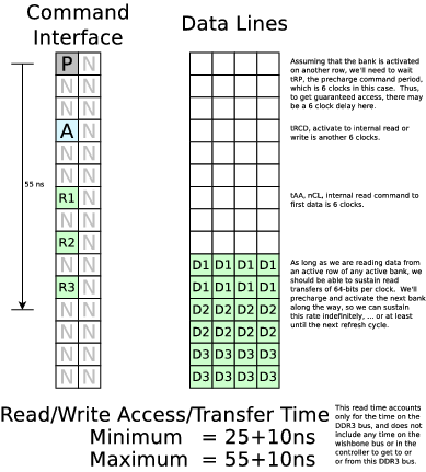
So I now need to retool this project (once again) for an 80MHz clock, and a 4:1 memory clock to system clock ratio. Going back to the DDR3 specification, that means our access times will be (5-5-5) (clocks at 320MHz). This will slow down our access time by about 2ns, and our transfer time down from 10ns/128bits down to 12.5ns/128bits.
Perhaps I'm trying to hard: what's 2.5ns between friends anyway?
At any rate, here are some updated memory read, memory write, and refresh timing diagrams.
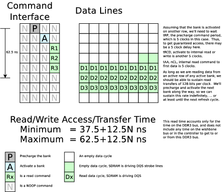 |
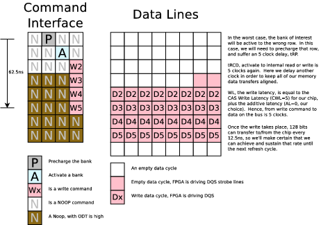 |
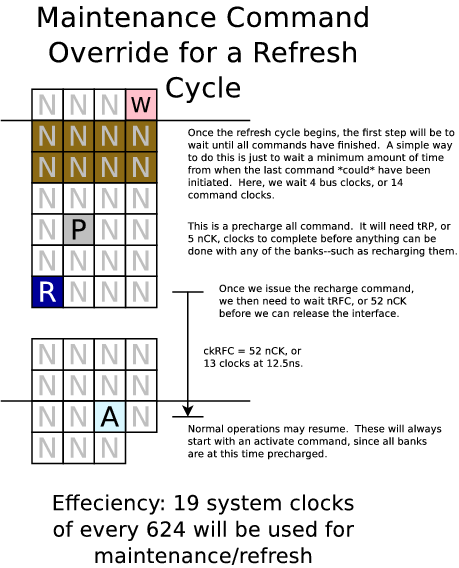 |
I expect it'll take a bit longer to get the Verilog code (and simulation) running with these new numbers, but that'll be my next step.
20160916 Update:
I was surprised to discover the other day that Xilinx's MIG will not build when given a clock at 100MHz and asked to run at 320MHz. It will only build for a 325MHz clock. Since Xilinx does their solution at 4:1, that makes their core run at an 81.25MHz clock.I then tried Xilinx's Memory Interface Generator core, and got it up and running using a simple bus translator. Much to my shock, their core requires about 24 clocks, at 81.25MHz, per transaction. (You can still see my testing work: it was done as part of the OpenArty project). Where did all this time go? You can see from our timing diagrams, that 9 clocks is more reasonable. The bus translator then adds a clock in the front, and two clocks at the end, leading to a 27 clock delay from strobe to ack. Need I say it again? This is pitiful!
So I got back to work today, and got the logic up and running, and passing all my simulator tests. While I'd like to say that it is now ready for the FPGA, it isn't. While the logic works in Verilator, and while it passes a fairly rigorous test suite, the source code has been so abused every time it has been "rewritten" that it really needs to be cleaned up first. There are variables in there that aren't used, variables that I don't know what they do, and more/worse. Once cleaned up though, it'll be time to head back to the FPGA and see if I can't get it running again.