
URL
https://opencores.org/ocsvn/virtex7_pcie_dma/virtex7_pcie_dma/trunk
Subversion Repositories virtex7_pcie_dma
Compare Revisions
- This comparison shows the changes necessary to convert path
/
- from Rev 42 to Rev 43
- ↔ Reverse comparison
Rev 42 → Rev 43
/virtex7_pcie_dma/trunk/README.md
0,0 → 1,50
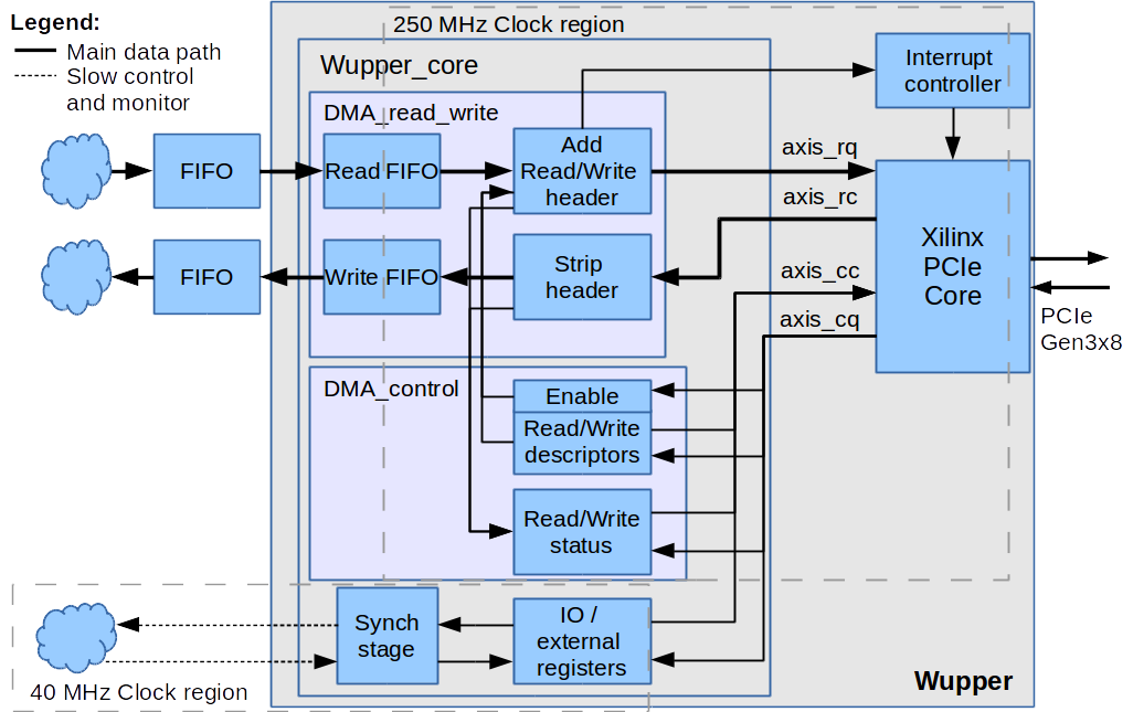
## Block Diagram |
|
 |
|
## Description |
|
Wupper is designed by [Nikhef](http://www.nikhef.nl) (Amsterdam, The Netherlands) for the CERN [ATLAS](http://atlas.cern) / [FELIX](https://atlas-project-felix.web.cern.ch/atlas-project-felix) project. |
Its main purpose is to provide a simple Direct Memory Access (DMA) interface to the Xilinx Virtex-7 PCIe Gen3 hard block. |
Wupper is specifically designed for the 256 bit wide AXI4-Stream interface of the [Xilinx Virtex-7 FPGA Gen3 Integrated Block for PCI Express (PCIe)](https://www.xilinx.com/products/intellectual-property/7_series_gen_3_pci_express.html). |
Wupper has been also successfully ported to Xilinx Kintex UltraScale FPGAs. |
|
#### DMA read and write |
|
The main purpose of Wupper is therefore to provide an interface to standard FIFOs. |
This is the done by the _DMA\_read\_write_ block in the diagram above. |
The read/write FIFOs have the same width as the Xilinx AXI4-Stream interface (256 bits) and run at 250 MHz. |
The application side of the FPGA design can simply read or write the FIFOs. |
Wupper will handle the transfer to Host PC memory, according to the addresses specified in the _DMA descriptors_. |
|
#### DMA control |
|
Another functionality of Wupper is thus to manage a set of DMA descriptors. |
Descriptors consist of an address, a read/write flag, the transfer size (number of 32 bit words) and an enable line. |
Descriptors are handled by the _DMA\_control_ block. |
These descriptors are mapped as normal PCIe memory or IO registers. |
Besides the descriptors and the enable line (one per descriptor), a status register for every descriptor is provided in the register map. |
|
#### Generic register map |
|
Besides DMA specific functions, the DMA control block can also handle generic _control_ and _monitor_ registers for user application. |
|
#### Interrupt handler |
|
Wupper is provided with a generic MSI-X compatible interrupt controller. |
|
#### Implementation info |
|
For synthesis and implementation of the cores, it is recommend to use Xilinx Vivado 2014.2. |
Other IP cores (FIFO, clock wizard and PCIe) are provided in the Xilinx .xci format, as well as the constraints file (.xdc) is in the Vivado 2014.2 Format. |
Wupper is also known to work well with Vivado 2014.4, constraints will be updated. |
|
For portability reasons, no Xilinx project files will be supplied with Wupper. |
Instead, a bundle of _TCL scripts_ has been supplied to create a project and import all necessary files, as well as to do the synthesis and implementation. |
These scripts are be described in details in the [/documentation/wupper.pdf](http://opencores.org/websvn,filedetails?repname=virtex7_pcie_dma&path=%2Fvirtex7_pcie_dma%2Ftrunk%2Fdocumentation%2Fwupper.pdf) distributed with Wupper. |
|
## Feedback |
|
|
\>> Give comments and feedback using the official core thread on the OpenCores forum: |
[forum\_thread](http://opencores.org/forum,Cores,0,5580) |