Bus Transaction Monitor with JTAG
Project maintainers
Details
Created: Mar 7, 2012
Updated: Feb 8, 2014
SVN Updated: Sep 23, 2014
SVN: Browse
Latest version: download (might take a bit to start...)
Statistics: View
Bugs: 2 reported / 1 solved
Other project properties
Language:Verilog
Development status:Beta
Additional info:FPGA proven
WishBone compliant: No
WishBone version: n/a
License: LGPL
TODO
To support Altera Qsys AXI4 Monitor IP integration.
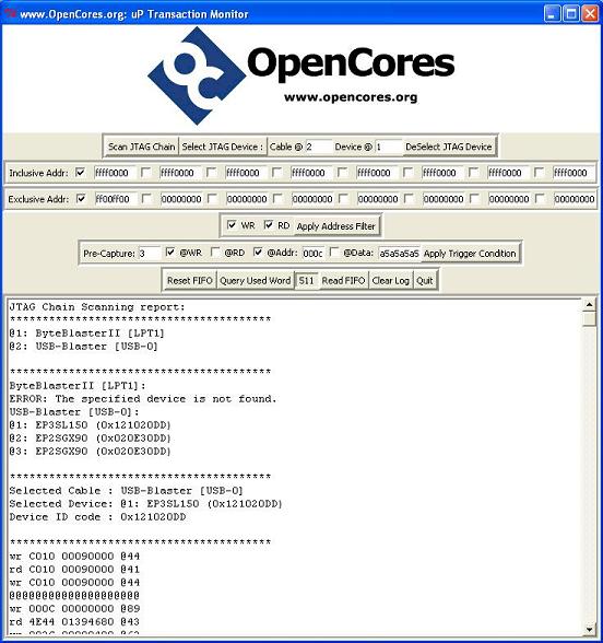
Tk GUI
Description
A CPU-to-FPGA bus transaction monitor, captures the CPU write/read address/data to/from memory-mapped registers that resides in the FPGA, and transmits the captured information to PC through JTAG download cable attached to the FPGA.
The detailed information about this low-level firmware debugger is published by the author on EDN.com as a Design Ideas article: Debug a microcontroller-to-FPGA interface from the FPGA side.
The original source code accompanying this article is set as the code base. Enhancements and additional features will be added.
Release 2.5 Added enhancements:
1. Capture address enlarged to 32bit.
Release 2.3 Added enhancements:
1. Xilinx FPGA support with ChipScope VIO. (In addition to Altera FPGA support with Virtual JTAG.)
2. AXI4-Lite Monitor as Xilinx Platform Studio IP.
Release 2.2 Added enhancements:
1. Multiple capture filter selection in the Tk GUI.
2. Read transaction capture.
3. Adjustable pre-trigger capture.
4. Capture content with transaction timing information.
Planned enhancements:
1. Parameterized RTL code for flexible implementation.
2. Comprehensive user guide for implementation and usage.

