
Pmod AD2 Driver
Project maintainers
Details
Created: Feb 11, 2025
Updated: Feb 13, 2025
SVN Updated: Feb 13, 2025
SVN: Browse
Latest version: download (might take a bit to start...)
Statistics: View
Bugs: 0 reported / 0 solved
Other project properties
Language:VHDL
Development status:Beta
Additional info:
WishBone compliant: No
WishBone version: n/a
License: LGPL
PmodAD2Driver
Pmod AD2 Driver for the 4 Channels of 12-bit Analog-to-Digital Converter AD7991. The communication with the ADC uses the I2C protocol. User can specifies the I2C Clock Frequency (up to 400 kHz with the Fast Mode).
Usage
User specifies inputs: I2C mode (i_mode), ADC Slave Address (i_addr), Configuration Byte (i_config_byte, write mode only) and the Last Read Cycle trigger (i_last_read, read mode only).
The i_enable signal can be triggered (set to '1') to begin transmission.
When started, the PmodAD2Driver executes the complete operation cycle (configurations or ADC conversions) independently of the new i_enable signal value.
At the end of the operation cycle, if the i_enable signal is still set to '1', the PmodAD2Driver executes the operation again with the current inputs.
The o_ready signal (set to '1') indicates the PmodAD2Driver is ready to process new operation. The o_ready signal is set to '0' to acknowledge the receipt.
The o_ready signal is set to '0' to acknowledge the receipt.
In Write mode, the PmodAD2Driver writes the Configuration byte into the ADC register and stop the transmission.
In Read mode, the PmodAD2Driver always reads 2-byte ADC conversion values channel-by-channel (according to ADC configuration).
The ADC value (o_adc_value) is available when its validity signal (o_adc_valid) is asserted.
In Read mode, while the i_last_read is NOT set to '1', the PmodAD2Driver execute the read operation.
ADC AD7991 has 2 I2C Addresses:
AD7991-0: 010 1000
AD7991-1: 010 1001
Configuration Register (8-bit Write Only):
| D7 | D6 | D5 | D4 | D3 | D2 | D1 | D0 | Bit |
|---|---|---|---|---|---|---|---|---|
| CH3 | CH2 | CH1 | CH0 | REF_SEL | FLTR | Bit Trial delay | Sample delay | Description |
| 1 | 1 | 1 | 1 | 0 | 0 | 0 | 0 | Default Value |
Configuration Register MSB Description:
| D7 | D6 | D5 | D4 | Analog Input Channel |
|---|---|---|---|---|
| 0 | 0 | 0 | 0 | No channel selected |
| 0 | 0 | 0 | 1 | Convert on VIN0 |
| 0 | 0 | 1 | 0 | Convert on VIN1 |
| 0 | 0 | 1 | 1 | Sequence between VIN0 and VIN1 |
| 0 | 1 | 0 | 0 | Convert on VIN2 |
| 0 | 1 | 0 | 1 | Sequence between VIN0 and VIN2 |
| 0 | 1 | 1 | 0 | Sequence between VIN1 and VIN2 |
| 0 | 1 | 1 | 1 | Sequence among VIN0, VIN1, and VIN2 |
| 1 | 0 | 0 | 0 | Convert on VIN3 |
| 1 | 0 | 0 | 1 | Sequence between VIN0 and VIN3 |
| 1 | 0 | 1 | 0 | Sequence between VIN1 and VIN3 |
| 1 | 0 | 1 | 1 | Sequence among VIN0, VIN1, and VIN3 |
| 1 | 1 | 0 | 0 | Sequence between VIN2 and VIN3 |
| 1 | 1 | 0 | 1 | Sequence among VIN0, VIN2, and VIN3 |
| 1 | 1 | 1 | 0 | Sequence among VIN1, VIN2, and VIN3 |
| 1 | 1 | 1 | 1 | Sequence among VIN0, VIN1, VIN2, and VIN3 |
Conversion Result Register (16-bit Read Only):
| D15 | D14 | D13 | D12 | D11 | D10 | D9 | D8 | D7 | D6 | D5 | D4 | D3 | D2 | D1 | D0 |
|---|---|---|---|---|---|---|---|---|---|---|---|---|---|---|---|
| 0 | 0 | CHID1 | CHID0 | MSB | B10 | B9 | B8 | B7 | B6 | B5 | B4 | B3 | B2 | B1 | B0 |
Signal Generator Pin Description
Generics
| Name | Description |
|---|---|
| sys_clock | System Input Clock Frequency (Hz) |
| i2c_clock | I2C Serial Clock Frequency (Standard Mode: 100 kHz, Fast Mode: 400 kHz) |
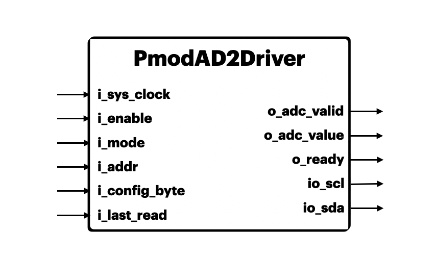
Ports
| Name | Type | Description |
|---|---|---|
| i_sys_clock | Input | System Input Clock |
| i_enable | Input | Module Enable ('0': Disable, '1': Enable) |
| i_mode | Input | Read or Write Mode ('0': Write, '1': Read) |
| i_addr | Input | ADC Address (7 bits) |
| i_config_byte | Input | ADC Configuration Byte (8 bits) |
| i_last_read | Input | Indicates the Last Read Operation ('0': Continue Read Cycle, '1': Last Read Cycle) |
| o_adc_valid | Output | ADC Read Value Valid ('0': Not Valid, '1': Valid) |
| o_adc_value | Output | ADC Read Value |
| o_ready | Output | ADC Ready Status ('0': NOT Ready, '1': Ready) |
| io_scl | In/Out | I2C Serial Clock ('0'-'Z'(as '1') values, working with Pull-Up) |
| io_sda | In/Out | I2C Serial Data ('0'-'Z'(as '1') values, working with Pull-Up) |