Spartan 6 PCIexpress card
Project maintainers
Details
Created: Mar 17, 2013
Updated: Aug 1, 2014
SVN Updated: Jul 28, 2014
SVN: Browse
Latest version: download (might take a bit to start...)
Statistics: View
Bugs: 0 reported / 0 solved
Other project properties
Language:VHDL
Development status:Beta
Additional info:
WishBone compliant: No
WishBone version: n/a
License: LGPL
Overview
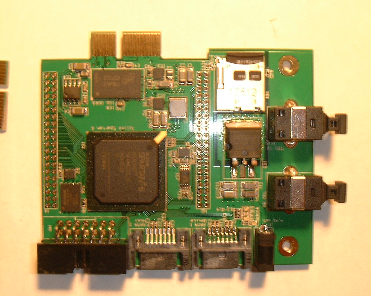
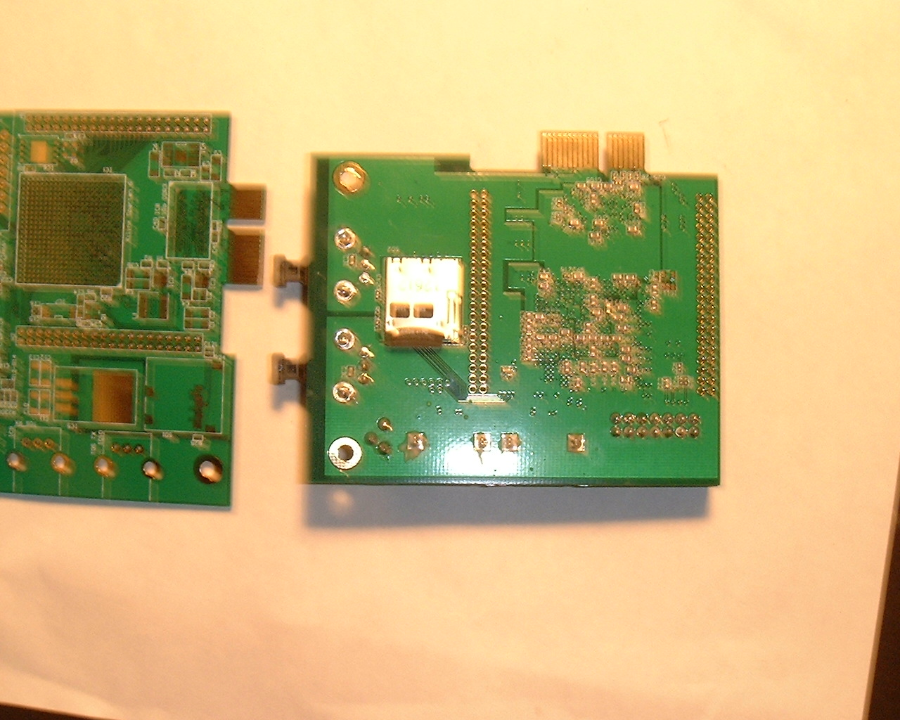
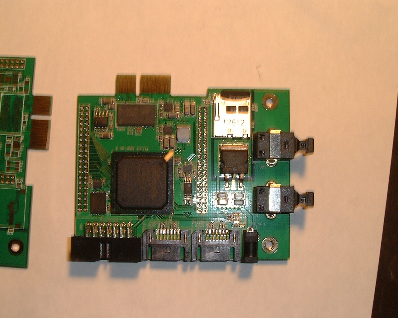
This article describe the PCI express card with Xilinx Spartan 6 that i have made.
The download section contains test applications in Xilinx ISE for the PCI express and DDR3 functions (All worked at first).
I am still not an expert so what would be more interesting (Processor core, intensive applications like running Linux ) is still a on wish list . PCB's are available as well as source project in Altium Designer.
Images
javascript:alert('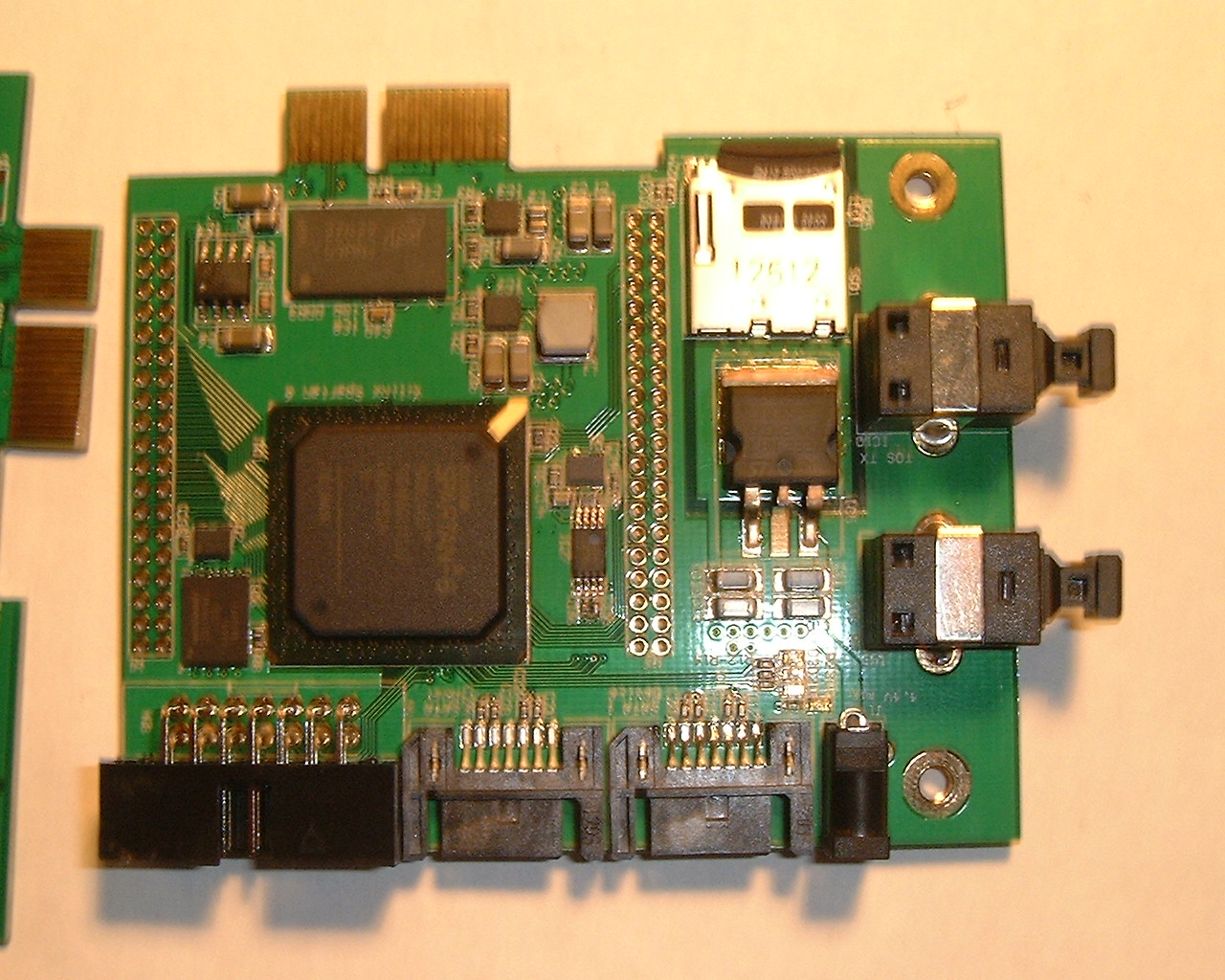
Part list
*All resistor and capacitor are 0603 if size not specified
*All resistor are either 0402 or 0603 size
*All capacitor are either 0402 or 0603 or 1206
*All components may be found on Mouser(1st choice) or Digikey , except FPGA and DDR3 Digikey only.
*DNF : means Do not fit (for example NCP303-LSN29 is not required for correct operation)
IC1 FPGA Xilinx XC6SLX45T-4FGG484C
IC2 VCCINT regulator ST1S31 (ST1S31PUR)
IC3 VDD15 regulator ST1S31 (ST1S31PUR)
IC4 RAM terminator VDD075 regulator LP2996 (LP2996MRX/NOPB)
IC5 VCC33 DC jack regulator LD1085 (LD1085D2T33R)
IC6 W25Q128 128Mbit Winbond flash memory (W25Q128FVEIG)
IC7 IDT ICS844071 SATA PLL (844071AGLF)
IC8 1Gbit Micron DDR3 DRAM MT41J64M16 (MT41J64M16JT-15E:G TR)
IC9 Everlight Photolink module PLR135_T7
IC10 Everlight Photolink module PLT135_T7
IC11 NCP303-LSN29 DNF
Q1 SATA 25Mhz Abracon ASEM or ASEMB 3.2x2.5x0.85
Q2 User 50Mhz Abracon ASEM or ASEMB 3.2x2.5x0.85
P1 PCIE card edge connector
H1,H2 double row 40pin 2.0mm header connector
J1 DC jack 3.5mm (Maybe found on Ebay..)
H3 14pin right angle 2.54mm JTAG connector
D1-D3 led 0603
D0 led 0603
SD1,SD2 500873-0806 Molex Transflash push-push
SATA1,SATA2 5607-4200-SH 3M SATA Connector SMT RA
L1 Inductor 2.2uH 4A Murata 2020 (LQH5BPN2R2NT0L)
L2 Inductor 3.3uH 1.1A 0806 Taiyo Yudan(CKP20163R3M-T)
R1 VCCINT_GND 15K
R2 VCCINT_PLUS 7.5K
R3 VDD15_GND 18K
R4 VDD15_PLUS 15.8K
R5,R6 100R output of sata crystal
R7 DO NOT FIT (can be 100R/0402 parallele resistor on pcie clock pair, but not nescessary)
R8 330R DONE to VCC33
R9 4K7 PROGRAM_B to VCC33
R10 10K CMPCS_B to VCC33
R11 4K7 INIT_B to VCC33
R12-R14 680R led resistor 0402
R15 240R 1% 0402 DRAM ZQ
R16 50R GTP RCAL 0402
R17-R18 4K7 0402 DDR CKE and Reset to GND
R19 10K SPI SS to VCC33 0402
R20 Swap enable 0R 0603
R21,R22 SD2 unused pins 22K 0402
R23 680R power led 0402
R24,R25 SD1 unused pins 22K 0402
R26,R27 pullup flash HOLD,WP 0402 10K
R28 IO_DDR_TERM calibration resistor 100R 0402
R29 DDR_CS tied to Gnd 0R 0402
C1 Capacitor1206 VCC33 to VCCINT switch input 100uF
C2 Capacitor1206 VCC33 to VDD15 switch input 100uF
C3,C3b Capacitor1206 VCCINT switch 100uF
C4 Capacitor1206 VDD15 switch 100uF
C5,C6 LP2996 100uF VDD075 output decoupl.
C7 LP2996 VREF decoupl. 10nF
C8 LP2996 VDD15 ref input decoupl. 10nF
C9 47uF 0805 VCC33 to LP2996 power input
C10,C11 50uF 1206 input to LD1085 regulator
C12,C13 100uF 1206 output of LD1085
C14 100nF output of SATA crystal
C15,C16 SATA REFCLK diff pair Capacitor0402 100nF
C17-C20 SATA1 RX/TX capacitor 0402 10nF
C21-C24 SATA2 RX/TX capacitor 0402 10nF
C25-C28 PCIE RX/TX capacitor 0402 100nF
C29 1nF NCP303
C30-C31 decoupling TOS RX/TX 100nF
C32 decoupling flash memory 100nF
C33 decoupling Q2 user 50Mhz oscillator(0402 size)
C34 decoupling Q1 sata 25Mhz oscillator(0402 size)
C35 decoupling SATA PLL ICS844071 (0603 size)
C40-C42 100nF VDD075 decoupling RAM
C45-C46 100nF VDD075 decoupling FPGA
C50-C56 1uF GTP decoupling
C60-C65 1uF VDD15 decoupling FPGA
C70-C74 1uF VCCINT decoupling
C80-C93 1uF VCCAUX/VCCO/VCC33 FPGA decoupling
C100-C109 1uF VDD15 decoupling RAM
C120 decoupling SD2 100nF 0402
C121 decoupling SD1 100nF 0402
Article
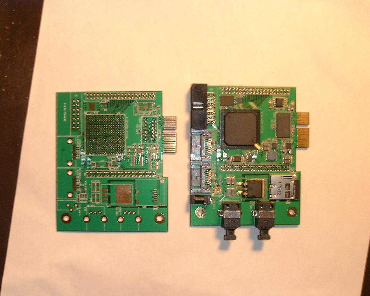
I have designed and built a PCI express extension card with Spartan 6 FPGA.
I was very attracted in testing Microprocessor cores in FPGA and also PC extension cards.
So i needed a board with RAM, non volatile memory (SDHC memory cards) and FPGA.
When i saw the selling price of this kind of cards, i decided to build mine. Also it was a good exercise to conduct the fabrication of this card from schematic and PCB up to assembling.
Many features where new to me:
-High speed differential pair
-Length matching and resistor terminations for DDR3
-big FPGA chips (DDR3 and FPGA)
So i have read carefully the design recommendation from the Manufacturers (Xilinx for FPGA and Micron for the DDR3). I got documented also on the Freescale IMX35 processor reference design . All recommended to carefully control PCB impedance , differential pair length matching, DDR3 signals length matching and termination resistors on high speed signals.
I had a new tool for PCB design (Altium designer) that made the task a lot easy or at least possible .
Anyway some problems came arise concerning the price of fine PCB manufacture:
First i designed a 8 layer PCB that accomplished impedance parameter of 50ohm on single ended signals and of course 100ohm on differential pairs. Moreover , the DDR signals where well separated each other with 2.5 x trace width that is recommended by Xilinx. But the PCB parameters where expensive to manufacture (traces of 0.1mm / vias of 0.4mm / 8 layers ) was 500USD cost for 10pcs.
I decided then to reduce cost , with only 4 layer (DDR traces where now shielded with only the top and bottom layer which are ground and power planes but with some discontinuity). Moreover i enlarged minimum trace width to become 0.15mm and via size to become 0.5mm.
With these parameters , impedance rule of 50R/100R is not really respected, also clearance between DDR signals is no 2.5 x trace width but only 2x trace width. Anyway , differential pair length matching is still stricly observed , also DDR length matching is also stricly observed with a total length of 26mm +- 0.2mm for all signals .
With these PCB parameters , the manufacture cost dropped to 120USD including a gold finish for all the contacts.
Finally , i received the PCB samples (they where of admirable perfect qualtity, i think the manufacturer have far better manufacture tolerance that it say) , assembled a board in 1 day and tested
1- The FPGA configuration and flash memory : Works perfectly in 1x and 2x SPI bus but no 4x bus , i currently don't konw why.
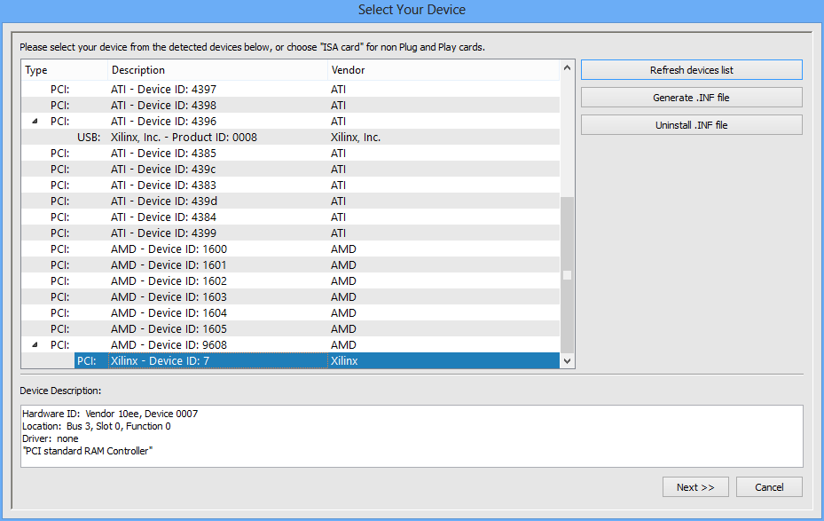
2- PCI express . Works perfectly . The Xilinx core generator automatically produce a sample core application that is a PCI express device of type 'RAM controller".
3- DDR3 : Works . Tests at 300Mhz clock (The core uses internally 2x this frequency using a PLL to double it).
Now many other things should be tested :
-SATA host and device connectors
-SDHC memory cards
-DDR3 and PCIE with a real intensive application . Like for example Linux why not!
The card is at my knowledge one of the first design not from a commercial company, and i propose the PCB for anyone interested. And also the Altium designer project source (PCB and schematic) in download section.
in case the PCB would be re - made , it would be a good idea to add a termination resistor on DRAM CLK differential pair. Yes it is not currently done, but it works! It could be still possible to solder it on the vias under the RAM chip.
DDR3 extensive test with Microblaze FPGA processor
I have learned what's required to setup microblaze on this board (processor running on Xilinx FPGA).
Many documentation can be found from Xilinx but also from AVNET .
A EDK licence is also required (Webpack free licence does not currently cover the full use of Xilinx SDK and Platform studio). By chance , they is a 30 day free evaluation licence for these products).
Setting up Microblaze is fairly fast and straightforward, nearly all project generation is automated with option wizards where you specify what's is on the target board. The result is a SDK project with commands like "Download microblaze to FPGA" and "Run or Debug application project". All of that is done with the JTAG cable connected.
I have specifically ran the DDR3 test application included with EDK basic application which extensively test the Memory by writing all the 128Mbyte memory locations then read and compare with expected value previously written. This test is performed with many flavor (Write constant value 0xFFFFFFFF,Write constant value 0x00000000,Write constant value 0xAAAA5555,Write incremented serie 1,2,3,..,0x0200000,Write inverse address as value,Write a rotated serie of 00..1..00 or 11..0..11.
Here is the a portion of the C application and the result shows that DDR3 on this card is working correctly .
Each run of writing and reading the 128Mbyte take approx 30s. The microblaze processor is clocked at 100Mhz.
int main()
{
int i;
init_platform();
print("--Starting Memory Test Application--\n\r");
print("NOTE: This application runs with D-Cache disabled.");
print("As a result, cacheline requests will not be generated\n\r");
for (i = 0; i < n_memory_ranges; i++) {
test_memory_range(&memory_ranges[i]);
}
print("--Memory Test Application Complete--\n\r");
cleanup_platform();
return 2;
}
--Starting Memory Test Application--
NOTE: This application runs with D-Cache disabled.As a result, cacheline requests will not be generated
Testing memory region: mcb_ddr3
Memory Controller: axi_s6_ddrx
Base Address: 0xc0000000
Size: 0x08000000 bytes
memtest words: 0x02000000 words
0xFFFFFFFF test: PASSED!
0x00000000 test: PASSED!
incr test: PASSED!
inverse addr test: PASSED!
0xAAAA5555 test: PASSED!
walk ones: PASSED!
walk zeros: PASSED!
--Memory Test Application Complete-
Running Linux on the board
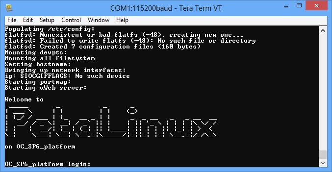
I have compiled a Petalinux kernel for this board.
See download section for instruction of how to do that.
The compilation results include a image.elf that is a Linux with and embedded RAM filesystem.
It is possible to setup various configurations based on Linux.
It is planned an expansion board with Ethernet, USB host , Serial and maybe VGA output.
Credit
PCB manufacturer for this card can be contacted at maisuid@gmail.com . dont hesitate to submit him your project for quote.
Project update
07-2014 . 3 new boards where built
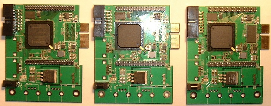
All worked properly without problem.
The feature tested where :
-FPGA, JTAG and Power supply
-Flash memory
-IO connectors, board leds and oscillator
-PCI express
-DDR3 (when installed)
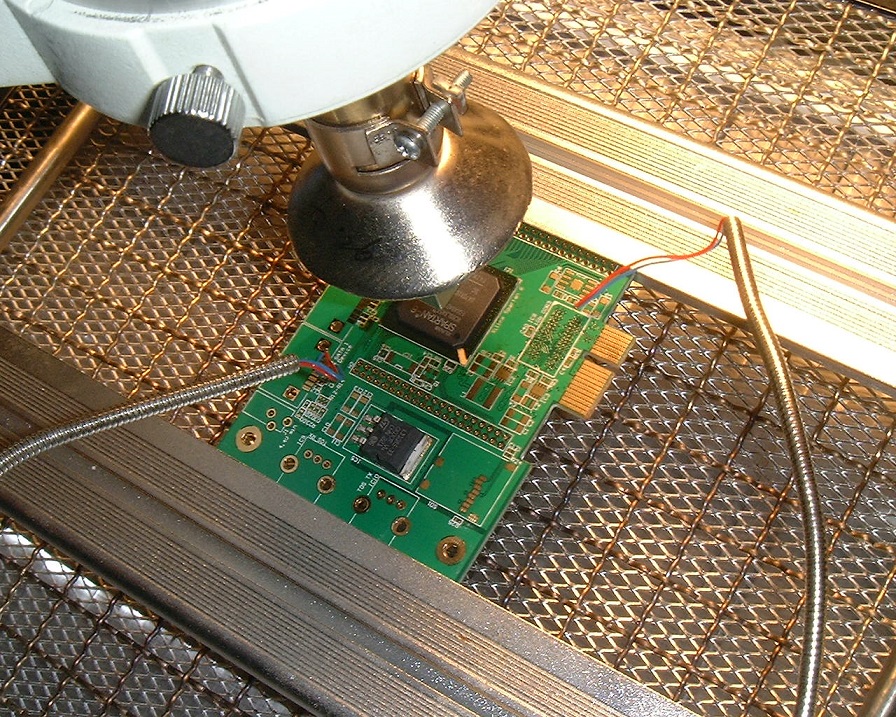
Example Linux / Windows drivers for PCIe where added to the download . An XPS design without Microblaze processor (only PCIe to peripherals bus) was added. Example PCIe drivers for Windows and Linux are proposed in Xilinx xapp1052. A "no driver" approach is possible with Jungo windriver under Windows and with open/mmap (on PCIe BAR resource) under Linux.
