 8/16/32 bit SDRAM Controller
Project maintainers
Details
Created: Jan 3, 2012
Updated: Apr 12, 2019
SVN Updated: Aug 27, 2021
SVN: Browse
Latest version: download (might take a bit to start...)
Statistics: View
Bugs: 5 reported / 3 solved
Other project properties
Language:Verilog
Development status:Stable
Additional info:Design done, Specification done
WishBone compliant: Yes
WishBone version: n/a
License: GPL
Description
Feature:
• 8/16/32 Configurable SDRAM data width
• Wish Bone compatible
• Application clock and SDRAM clock can be async
• Programmable column address
• Support for industry-standard SDRAM devices and modules
• Supports all standard SDRAM functions
• Fully Synchronous; All signals registered on positive edge of system clock
• One chip-select signals
• Support SDRAM with four bank
• Programmable CAS latency
• Data mask signals for partial write operations
• Bank management architecture, which minimizes latency
• Automatic controlled refresh
• Static synchronous design
• Fully synthesizable
This project is used IITM shakti project and you can see the same source code at
https://gitlab.com/shaktiproject/uncore/devices/tree/master/sdramcontroller
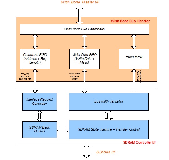
Functional Block Diagram
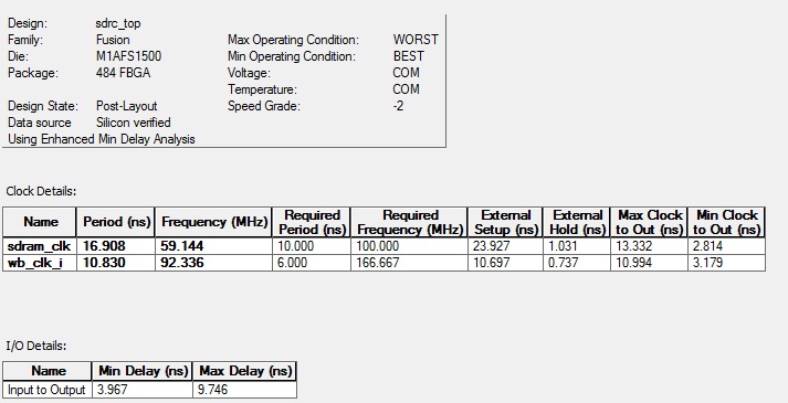
FPGA bench Mark
Status
Stable RTL ver 0.1 is available
Frequently Asked Question
1. Design and implementation language used in the IP
Design implementation is done Verilog and System verilog language
2. What are the SDRAM Bus width are supported by the IP?
This IP Supports 8/16/32 Bit interface
3. What are the Application Bus width are supported by the IP?
This IP Supports only 32 bit Application Bus width
4. Can Application clock and SDRAM clock be Asynchronous to each other?
Yes, IP support both Synchronous and Asynchronous Application clock and SDRAM clock
5.Is the application layer is compatible to wish-bone standard?.
Yes, Application Layer is wishbone compatible.
6.Is SDRAM cores is also available with custom interface?
Yes. SDRAM core is separately available with automated test-bench.
7.Test bench scripts are compatible to which tool?
Verification scripts are compatible to model simulator


