
A VHDL 6532 RIOT
Project maintainers
Details
Name: vhdl_6532_riot
Created: Mar 29, 2018
Updated: Mar 30, 2018
SVN Updated: Mar 30, 2018
SVN: Browse
Latest version: download (might take a bit to start...)
Statistics: View
Bugs: 0 reported / 0 solved
Created: Mar 29, 2018
Updated: Mar 30, 2018
SVN Updated: Mar 30, 2018
SVN: Browse
Latest version: download (might take a bit to start...)
Statistics: View
Bugs: 0 reported / 0 solved
Star2you like it: star it!
Other project properties
Category:Other
Language:VHDL
Development status:Stable
Additional info:Design done, FPGA proven, Specification done
WishBone compliant: No
WishBone version: n/a
License: Others
Language:VHDL
Development status:Stable
Additional info:Design done, FPGA proven, Specification done
WishBone compliant: No
WishBone version: n/a
License: Others
Description
VHDL implementation of the 6532 RIOT (RAM-I/O-TIMER)

The R6532 integrates several functions:
- RAM (128 x 8)
- Two parallel I/O ports
- Timer functions
- Interrupt capabilities
Signal interface
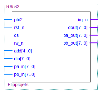
phi2 : The clock signal. Should be connected to the CPU's Phi2 line.
rst_n : The reset signal (negative). Should be connected to the CPU's RST line.
irq_n : The interrupt line (negative). Should be connected to CPU's IRQ or NMI, if needed.
rw_n : The read/write signal (Read = 1, Write = 0). Should be connected to the CPU's R/W line.
cs : Chip select (positive). Should be connected to the address decoding logic.
add[4..0] : Address bus. Should be connected to the CPU's address bus.
din[7..0] : Data bus, inputs. Connected to the CPU data bus outputs.
dout[7..0] : Data bus, outputs. Connected to the CPU data bus inputs (need multiplexers)
pa_in[7..0] : Port A, inputs.
pa_out[7..0] : Port A, outputs.
pb_in[7..0] : Port B, inputs.
pb_out[7..0] : Port B, outputs.
Tests and validation
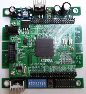
The R6532 component has been tested on an ALTERA Cyclone IV FPGA - EP4CE6 (and EP4CE10).It was used in our Gottlieb pinball sound card replacement project, that integrate a 6502 core, RAM, ROM and R6532/R6530 devices.
The board C4E6-K (or C4E10-K) is clocked at 50 MHz, the 6502 core run at 892 Khz.
Registers
Refer to the original documentation of this chip for registers description.The only difference is that this implementation use a single cs signal for selection. No need of CS1, CS2, RS, nor A5..A6, as the RAM is not implemented.
© copyright 1999-2018 OpenCores.org, equivalent to Oliscience, all rights reserved. OpenCores®, registered trademark.