
 Wupper: PCIe DMA Engine for Xilinx FPGAs
Project maintainers
Partner team

Details
Created: Dec 18, 2014
Updated: Mar 27, 2024
SVN Updated: Sep 10, 2021
SVN: Browse
Latest version: download (might take a bit to start...)
Statistics: View
Bugs: 11 reported / 10 solved
Other project properties
Language:VHDL
Development status:Mature
Additional info:Design done, FPGA proven, Specification done
WishBone compliant: Yes
WishBone version: B.4
License: Others
Wupper: A PCIe Gen3/Gen4/Gen5 DMA controller for Xilinx FPGAs.
The repository was moved to Nikhef Gitlab. Gitlab is expected to land on Opencores as well, until then Nikhef will be used.
Please visit: https://gitlab.nikhef.nl/franss/wupper/
The Opencores page will be maintained to keep the project together
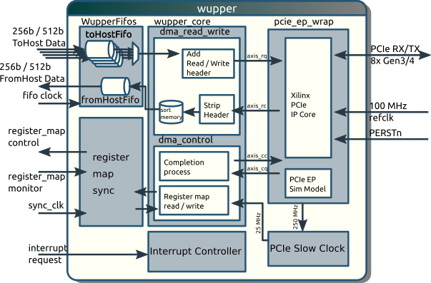
Block Diagram
Description
Wupper is designed by Nikhef (Amsterdam, The Netherlands) for the CERN ATLAS / FELIX project. Its main purpose is to provide a simple but high performance Direct Memory Access (DMA) interface to the Xilinx Virtex-7 PCIe Gen3 hard block and later series. Wupper is specifically designed for the 256/512/1024 bit wide AXI4-Stream interface of the Xilinx Virtex-7 FPGA Gen3 Integrated Block for PCI Express (PCIe). Wupper has been also successfully ported to Xilinx Kintex UltraScale, Virtex Ultrascale+, Versal Prime and Versal Premium FPGAs, supporting PCIe Gen3, Gen4 and Gen5.
DMA read and write
The main purpose of Wupper is therefore to provide an interface to standard FIFOs. This is the done by the DMA_read_write block in the diagram above. The read/write FIFOs have the same width as the Xilinx AXI4-Stream interface (256 bits for PCIe Gen3 and 512 bits for PCIe Gen4 inter) and run at 250 MHz. The application side of the FPGA design can simply read or write the FIFOs. Wupper will handle the transfer to Host PC memory, according to the addresses specified in the DMA descriptors.
DMA control
Another functionality of Wupper is thus to manage a set of DMA descriptors. Descriptors consist of an address, a read/write flag, the transfer size (number of 32 bit words) and an enable line. Descriptors are handled by the DMA_control block. These descriptors are mapped as normal PCIe memory or IO registers. Besides the descriptors and the enable line (one per descriptor), a status register for every descriptor is provided in the register map.
Generic register map
Besides DMA specific functions, the DMA control block can also handle generic control and monitor registers for user application. The registers are maintained in a .yaml file and python scripts are provided to convert them into VHDL, C and LaTeX.
Interrupt handler
Wupper is provided with a generic MSI-X compatible interrupt controller.
Implementation info
- For synthesis and implementation of the cores, it is recommend to use Xilinx Vivado 2023.2.
- Other IP cores (clock wizard and PCIe) are provided in the Xilinx .xci format, as well as the constraints file (.xdc) is in the Vivado 2023.2 Format, FIFO cores are using XPM macros.
- For Versal devices, Vivado 2020.1 is used as well, but there may be better support in later Vivado editions. We will upgrade later.
- The Virtex Ultrascale+ VU9P works with PCIe Gen4 however this was officially dropped by Xilinx. To use these devices with Gen4, Vivado 2018.1 has to be used.
For portability reasons, no Xilinx project files will be supplied with Wupper. Instead, a bundle of TCL scripts has been supplied to create a project and import all necessary files, as well as to do the synthesis and implementation. These scripts are be described in details in the /documentation/wupper.pdf distributed with Wupper.
Feedback
>> Give comments and feedback using the official core thread on the OpenCores forum: forum_thread